Patterned nanomagnets
DOI: 10.1063/1.2754602
A magnet has two poles, as any child can tell you. However, the familiar dipole configuration is not the only one that a magnet can have. The configuration of any magnet is the result of several competing energies: the exchange energy of interaction among the atomic moments, the magnetostatic energy of the magnetic field itself, and the magnetocrystalline anisotropy energy. The relative importance of each of the three energies depends on the size, shape, and material properties of the magnet.
The exchange interaction is what causes magnetic ordering in the first place. The most common representation of exchange energy is the Heisenberg interaction of
One of the best venues to explore the range of possible configurations is in patterned nanomagnets with well-defined shapes in the submicron size range. 1 The exchange and magnetostatic energies in that regime are of similar magnitude, so small variations in size and shape can shift the energy balance between the exchange energy, which favors parallel alignment of the magnetic moments, and the magnetostatic energy, which promotes magnetic closure structures with no stray magnetic field. (For simplicity, we assume the magnetocrystalline anisotropy energy to be negligible.) Many of the resulting configurations are unseen in either soft or hard macroscopic magnets. Patterned nanomagnets are central to many magnetic technologies, such as magnetic recording read heads 2 already in use and magnetoresistive random access memory (MRAM) 3 still being developed. In such applications the proper choices of size and shape of the nanomagnets are essential in capturing the unique magnetoelectronic properties.
The studies of the spin configurations and the intriguing phenomena in nanomagnets require advanced fabrication, imaging, and measurement techniques together with theoretical understanding and micromagnetic simulations. Many revealing results have only become available during the past few years. In this article we concentrate mainly on circular nanomagnets, but nanomagnets can have various shapes, including spheres, wires, tubes, disks, and rings. Fabrication methods must produce nanomagnets with well-defined shapes and sizes and with smooth sidewalls. The magnetic configurations can be imaged by spin-sensitive microscopies, such as magnetic force microscopy (MFM) and x-ray microscopy.
Single-domain state
The exchange energy is minimized when all the moments are aligned to form the single-domain state, shown in figure 1a, with a saturation magnetization M S and a dipole moment of µ = M S V, where V is the volume of the nanomagnet. Any deviation from parallel alignment increases the exchange energy with an energy density proportional to both the strength of the exchange interaction and the square of the magnetization gradient. Other important lengths are l ex, the length scale of the exchange interaction, and δ w, the domain-wall width. For most soft magnets, l ex is a few nanometers and δ w is a few times l ex. In flat nanomagnets with a thickness of about l ex, there is little magnetic variation within the thickness. The magnetic configuration at the surface is the same as the configuration within the disk.

Figure 1. Configurations of patterned nanomagnets. (a) A circular disk in the single-domain state, in which all the magnetic moments are parallel, generates a magnetic field in its vicinity, which contributes to the magnetostatic energy. (b) The vortex state has no stray magnetic field, but the exchange energy of interaction among the moments (white arrows) is nonzero. (c) The vortex core, a small region in which the moments align perpendicular to the plane of the disk, decreases the exchange energy at the center of the vortex. (d) Square disks can also acquire a vortex state, with four domains and four domain walls that intersect at the vortex core. (e) A vortex pair can be formed in an elliptical disk. (f) The two vortex cores, at the intersections of the thin black lines, move with respect to each other (red arrows) in response to an applied magnetic field H (black arrows).

For very small nanomagnets with dimensions of a few tens of nanometers, the exchange energy dominates and the single-domain state is energetically preferred. In larger nanomagnets, the single-domain state is replaced by other configurations dependent on the shape of the magnet. For circular disks, the single-domain state is succeeded by the vortex state.
Vortex state
Consider a thin circular disk of diameter D and with thickness t much less than D. The magnetostatic energy of the single-domain state increases with the disk dimensions. In the vortex state, shown in figure
The otherwise perfect vortex arrangement is altered because of the large exchange energy density near the singularity at the vortex center. It is energetically favorable for the magnetic moments within a small central region, called the vortex core, to revolt and align perpendicular to the disk plane, as shown in figure
Square disks of similar size also adopt a vortex state, shown in figure
Vortex structures have been observed by several different techniques, such as MFM, 6 photoemission electron microscopy, 7 and electron holography. Most of the techniques have either vertical or in-plane contrast but not both: MFM can detect the polarity of the vortex core but not the chirality of the vortex, whereas PEEM can detect the chirality of the vortex but not the polarity of the core. The various techniques reveal the intricate physics of the vortex state over the limited size range in which it exists.
Vortex dynamics
Figure 2 depicts the response of circular magnets to an applied magnetic field. At zero field, a 200-nm permalloy disk is in the vortex state, and the in-plane magnetization is zero. When a small magnetic field is applied, the portion of the vortex with spins parallel to the field expands, and the vortex moves perpendicular to the field. A counterclockwise vortex moves to the left as viewed in the direction of the field, and a clockwise vortex moves to the right. There is a concomitant increase in magnetization linearly dependent on the applied field H. The movement of the vortex continues until the vortex core reaches the edge of the disk and disappears at the annihilation field H A, at which M abruptly increases. A slightly larger field beyond H A aligns the disk into the single-domain state. When the applied field is then reduced, the core does not reappear until H reaches the nucleation field H N, at which point the magnetization drastically decreases. The new vortex may or may not have the same chirality as the original vortex. The values of H N and H A depend strongly on the size, thickness, material, and defect density of the disk; a representative range for H A is 0.05–0.3 T. The nucleation field H N can even be negative for small disks, as shown by the red curve in figure 2.

Figure 2. A micromagnetic simulation of the hysteresis loops of circular nanomagnets in response to an applied magnetic field. A disk with a diameter D of 200 nm (blue) is in the vortex state at zero field, and the magnetization M is zero. The field H shifts the vortex reversibly to the left or to the right. At large enough H, the disk enters the single-domain state, with M equal to the saturation magnetization M S, at which point the dynamics are irreversible. A smaller disk (red) that is in the single-domain state at zero field exhibits slightly different behavior.

Within the field range −H A < H < +H A, the motion of the vortex core is reversible. The changing magnetostatic energy provides a restoring force, analogous to that of a Hooke’s-law spring, that pulls the vortex core back toward the center of the disk. The initial susceptibility, M/H, provides a measure of the stiffness of the sideways movement of the core. If the vortex core is rigid, its displacement is proportional to H. 8
The direction of the vortex core’s motion under a DC magnetic field reveals only the chirality of the vortex, not the polarity of the core. However, in response to an AC magnetic field of small amplitude, the vortex core not only oscillates but also executes a circular motion known as gyration. The gyrovector G of the vortex core is defined as −(2π ptM S/γ)z, where p is the polarity of the vortex core, t is the thickness, M S is the saturation magnetization, γ is the gyromagnetic ratio, and z is the unit vector perpendicular to the disk. The gyrotropic force on the vortex core is G × v, where v is the velocity of the vortex core. Because the effective mass of the vortex core is small, the core’s trajectory is determined by the balance of the gyrotropic force and the magnetostatic restoring force described previously. 9
The direction of the gyrotropic force with respect to the velocity is independent of the vortex chirality and depends only on the core polarity or, more formally, on the topological invariant known as the skyrmion number, which is +
Reversing the vortex core’s polarity by applying a magnetic field perpendicular to the disk requires a large field of about 0.3 T. Bartel Van Waeyenberge and colleagues 11 recently demonstrated that the core polarity can also be reversed by a pulsed in-plane field of only 1.5 mT, a useful technique that facilitates the use of the vortex core to store information. The process involves the creation of a new vortex–antivortex pair with like polarities opposite to the original vortex. The subsequent annihilation of the old vortex and the antivortex changes the total skyrmion number, and thus produces a burst of spin waves as described in the box. 11 , 12
Two vortices can be created in an elliptical disk,
13
as shown in figure
The skyrmion number of vortices and antivortices
A vortex or antivortex with winding number n and core polarity p has a half-integer skyrmion number q = np/2. The winding number, or vorticity, is +1 for a vortex, regardless of the clockwise or counterclockwise chirality, and −1 for an antivortex; more generally, it is the change in the angle of the local magnetization, integrated over a loop around the vortex core and divided by 2π. The winding number and the skyrmion number are both conserved during a continuous deformation of the magnetic configuration. For a vortex–antivortex pair of like polarity, the total winding number and the total skyrmion number are both zero. Such a pair is topologically equivalent to the single-domain configuration, so the pair can be created or annihilated through a continuous deformation. In contrast, a vortex–antivortex pair of opposite polarity has a nonzero skyrmion number, so the annihilation of such a pair produces a violent burst of spin waves.

Nanorings
The topological difference between a nanoring and a circular disk is reflected in the differences in their properties. The vortex core, which has such influence over the dynamics of a circular disk, is absent in a nanoring, as long as the ring width is less than the domain-wall width of about 50 nm. Most nanorings reported to date, with diameters between 0.5 and 5 µm, have been made by electron-beam lithography. 14 Template lithography, shown in figure 3, allows the fabrication of smaller nanorings with diameters of 100 nm and ring widths of 20 nm. 15

Figure 3. Fabrication of nanorings by template lithography. (a) Polystyrene nanospheres 100 nm in diameter are attached to a substrate. (b) A thin film of metal is deposited onto the surface. An argon-ion beam etches away the film at (c) normal incidence or at (d) oblique incidence. Scanning electron microscopy can be used to image the resulting (e) symmetric nanorings and (f) asymmetric nanorings.
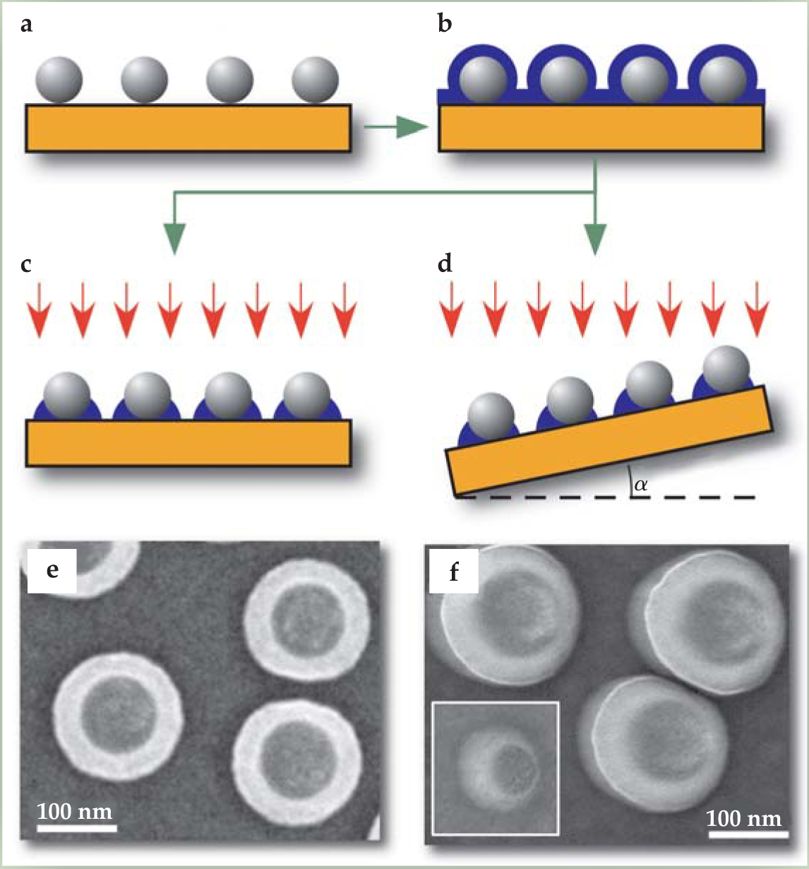
In the first step in template lithography, monodisperse nanospheres, such as 100-nm polystyrene spheres, are attached to a substrate by chemical means. A metal film is then deposited over the entire surface, including the regions below the nanospheres. An argon-ion beam at normal incidence etches away all materials except those protected under the spheres. The resulting nanorings have tapered cross sections. The diameter and number density of the nanospheres determine those of the nanorings. The thickness of the nanorings, measured perpendicular to the plane, can be as much as the radius of the nanospheres.
In the remanent state at zero field (after being magnetized with a large magnetic field), a nanoring acquires the so-called onion state, shown in figure 4, in which two semicircular domains are separated by two domain walls 180° apart. The two domain walls can also be viewed as two poles. When a magnetic field is applied opposite to the nanoring’s magnetization, the two domain walls move, with two possible routes. In the vortex process, shown in figure

Figure 4. Nanoring dynamics in response to an applied magnetic field. Micromagnetic simulations of (a) the vortex process, in which the two domain walls move toward each other, and (b) the onion-rotation process, in which the two domain walls move in tandem. In the inset of (a), half vortices of vorticity +
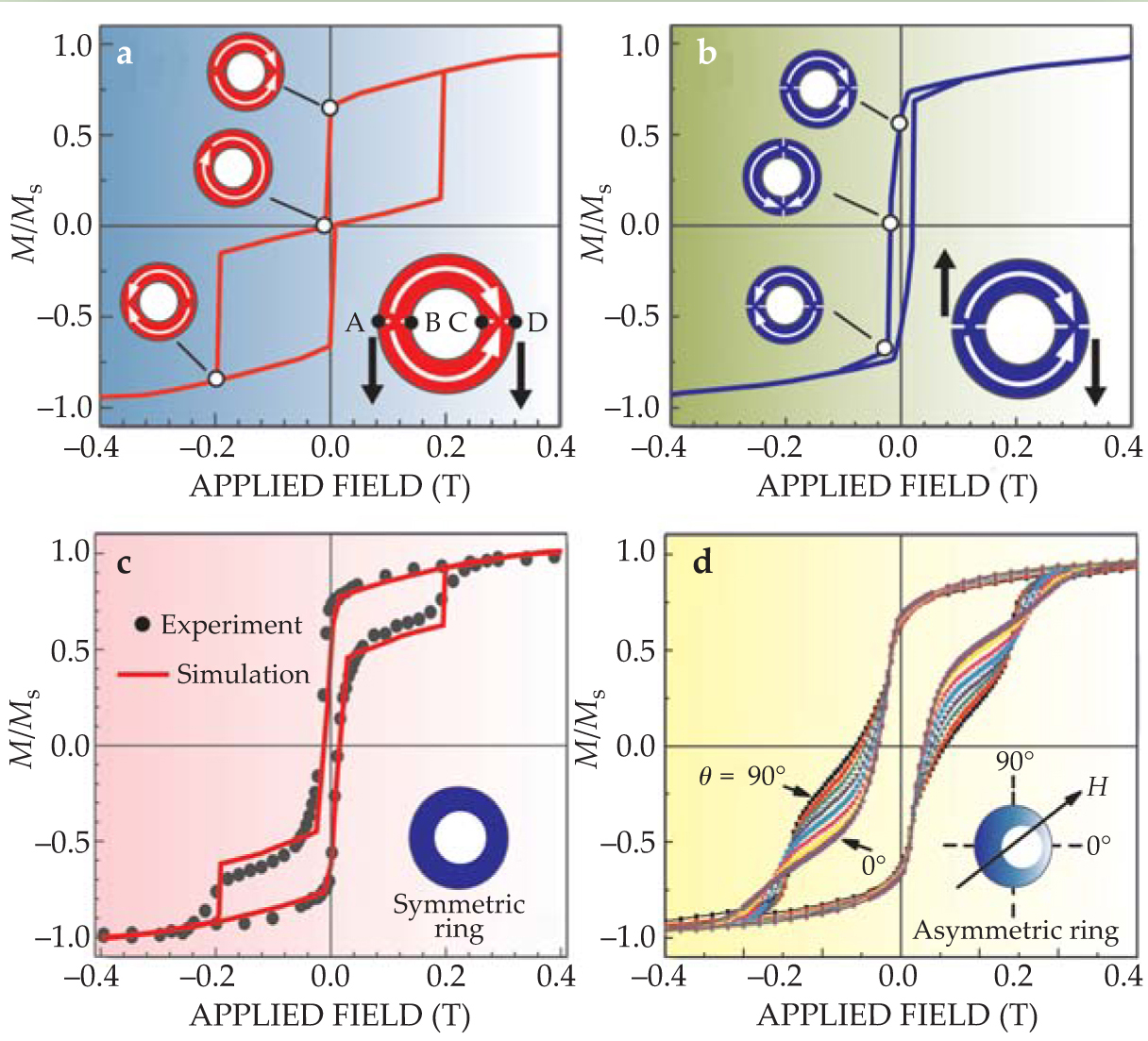
Alternatively, in the onion-rotation process, the two domain walls move in tandem and maintain their 180° separation, as shown in figure
The vortex state of a nanoring also has two chiralities. In symmetric nanorings, which have a uniform cross section along the circumference, both vortex chiralities are equally likely to be formed during the vortex process. The switching behavior of the symmetric nanorings is isotropic, independent of the direction of the in-plane magnetic field. Theory and simulations have suggested that a domain wall tends to move toward a region of reduced cross section. That tendency has been observed in asymmetric nanorings, in which one side is wider and thicker than the other. The asymmetric nanorings are made by the same template fabrication process, but with the argon-ion beam incident at an oblique angle, as shown in figure
Asymmetric rings have in-plane anisotropy. Their switching behavior depends on the direction θ of the initial magnetic field. Within the plane of the rings, the symmetry axis is defined such that the thinnest point of the ring is at θ = 0° and the thickest is at θ = 180°. For rings approximately 100 nm in diameter, the fraction of rings that undergo the vortex process increases from 40% at θ = 0° to essentially 100% at θ = 90°, at which point the two domain walls in the onion state nearly always move toward the side of the ring with the smaller cross section.
16
Representative hysteresis loops are shown in figure
In the vortex process, the vortex is created by the annihilation of two domain walls. That annihilation is possible only if the nanoring is sufficiently thick. Each of the two domain walls can be treated as a combination of two half vortices:
12
one on the outer edge of the ring with winding number −
Applications
Nanomagnets feature prominently in a number of applications, including read heads 2 and MRAM. 3 The nanomagnets in those devices must perform reliably and controllably in response to magnetic fields and electric currents. Circular-disk magnets have mostly been avoided because of the various configurations they can adopt. Instead, most applications use nanomagnets of an oblong shape in which the magnetostatic energy causes the magnetic moments to align along the long axis to create two definite orientations. The unique attributes of nanorings offer new prospects.
Whereas a read head is a single device, MRAM is an array of a large number of memory units, each of which must be individually addressed and accessed. The giant magnetoresistive (GMR) effect and, more recently, the tunneling magnetoresistive effect enable direct electronic readout from multilayer nanomagnet structures. 17 The multilayer contains two magnetic layers: the storage layer, which can be switched between two definite magnetic states, and the reference layer, which is kept in one particular state. Separating the storage and reference layers in GMR devices is a thin metallic layer; in magnetic tunnel junctions, the intervening layer is an insulator that acts as a barrier for spin-dependent quantum tunneling between the two magnetic layers. MTJs are appealing because they have a higher impedance than GMR devices; what is more important, they have an extremely high magnetoresistance ratio, defined as the percent difference in the resistance between the states in which the magnetizations of the two magnetic layers are parallel and antiparallel to each other. Magnetoresistance ratios of more than 400% at room temperature have been observed in MTJs that use crystalline magnesium oxide as a tunnel barrier between cobalt- or iron-based magnetic layers, with the crystalline structures of the layers epitaxially matched at the interfaces. 18
The first generation of MRAM, now commercially available with a capacity of 4 Mbits, employs two large currents to generate the necessary magnetic fields for switching a specific MTJ. That scheme of switching from a distance is not scalable, because for very small MTJs the switching field spills over into neighboring cells, so the prospects for using the scheme in high-density memories are limited. However, the high spin polarization in the MgO-based MTJs is well suited for spin-torque-driven switching, in which the magnetization is switched by passing a current of spin-polarized electrons through the MTJ. That switching scheme can more readily target the desired MTJ with no effect on its neighbors, and the required amplitude of the switching current is small when the size of the MTJ is in the range of 100 nm.
The dependence of magnetic-switching behavior on the shape of a nanomagnet may hold the key to the miniaturization of MRAM. In the oblong memory elements currently in use, any geometric, morphological, or physical variations of the tapered ends and along the edges of the elements can cause significant changes in the switching-field threshold. An alternative is to use ring-shaped memory elements, shown in figure 5a. The nanoring geometry not only eliminates sharp ends but also requires a much smaller switching current.

Figure 5. Nanoring magnetic tunnel junctions for use in magnetoresistive random-access memory. (a) The MTJ consists of a storage layer and a reference layer separated by an insulating layer. The magnetic configuration of the reference layer is kept constant. Switching the storage layer between two available states, representing 1 and 0, changes the electrical resistance of the cell. Three schemes have been proposed for the configurations of the storage and reference layers: (b) both layers in the onion state, (c) both layers in the vortex state, and (d) the reference layer in the vortex state and the storage layer in the twisted state. (e) The state of the storage layer can be switched by a current of spin-polarized electrons.
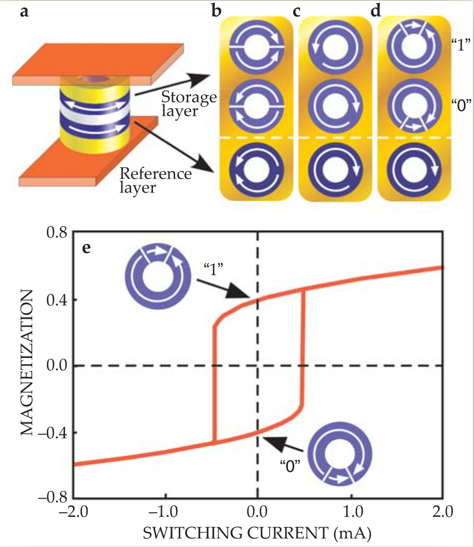
Several schemes for nanoring MTJs have been proposed. In the first scheme, the reference layer and the storage layer are both in the onion state. The two orientations of the onion state shown in figure
A more advantageous scheme, shown in figure
The rich and fascinating phenomena exhibited by nanomagnets depend intricately on the magnets’ shape and size. The engineering of patterned nanomagnets with well-defined memory states and robust, repeatable, and uniform magnetic switching characteristics is a fertile area for exploring future magnetic and magnetoelectronic devices. As vividly displayed by the examples above, although the dipole configuration is a familiar and useful state that a magnet can acquire, it is certainly not the most interesting one.
We are grateful to many colleagues whose advances have made patterned nanomagnets such a vibrant, exciting, and technologically relevant field. We thank Xiaochun Zhu of Carnegie Mellon University for useful exchanges and Oleg Tchernyshyov of the Johns Hopkins University for illuminating discussions and critical reading of this manuscript. We thank NSF for supporting our research.
References
1. S. D. Bader, Rev. Mod. Phys. 78, 1 (2006). https://doi.org/10.1103/RevModPhys.78.1
2. J. -G. Zhu, Mater. Today 6(7–8), 22 (2003). https://doi.org/10.1016/S1369-7021(03)00729-6
3. J. -G. Zhu, C. Park, Mater. Today 9(11), 36 (2006). https://doi.org/10.1016/S1369-7021(06)71693-5
4. R. P. Cowburn et al., Phys. Rev. Lett. 83, 1042 (1999). https://doi.org/10.1103/PhysRevLett.83.1042
5. A. Wachowiak et al., Science 298, 577 (2002). https://doi.org/10.1126/science.1075302
6. T. Shinjo et al., Science 289, 930 (2000). https://doi.org/10.1126/science.289.5481.930
7. S. -B. Choe et al., Science 304, 420 (2004). https://doi.org/10.1126/science.1095068
8. K. Y. Guslienko et al., Phys. Rev. B 65, 024414 (2002). https://doi.org/10.1103/PhysRevB.65.024414
9. K. Y. Guslienko et al., Phys. Rev. Lett. 96, 067205 (2006). https://doi.org/10.1103/PhysRevLett.96.067205
10. T. Senthil et al., Science 303, 1490 (2004). https://doi.org/10.1126/science.1091806
11. B. Van Waeyenberge et al., Nature 444, 461 (2006). https://doi.org/10.1038/nature05240
12. O. A. Tretiakov, O. Tchernyshyov, Phys. Rev. B 75, 012408 (2007); https://doi.org/10.1103/PhysRevB.75.012408
O. Tchernyshyov, G.-W. Chern, Phys. Rev. Lett. 95, 197204 (2005). https://doi.org/10.1103/PhysRevLett.95.19720413. K. S. Buchanan et al., Nat. Phys. 1, 172 (2005). https://doi.org/10.1038/nphys173
14. M. Kläui, C. A. F. Vaz, L. Lopez-Diaz, J. A. C. Bland, J. Phys.: Condens. Matter 15, R985 (2003); https://doi.org/10.1088/0953-8984/15/21/201
C. A. Ross et al., J. Appl. Phys. 99, 08S501 (2006). https://doi.org/10.1063/1.216560515. F. Q. Zhu et al., Adv. Mater. 16, 2155 (2004). https://doi.org/10.1002/adma.200400675
16. F. Q. Zhu et al., Phys. Rev. Lett. 96, 027205 (2006). https://doi.org/10.1103/PhysRevLett.96.027205
17. G. A. Prinz, Science 282, 1660 (1998). https://doi.org/10.1126/science.282.5394.1660
18. S. Yuasa et al., Appl. Phys. Lett. 89, 042505 (2006). https://doi.org/10.1063/1.2236268
More about the authors
Chia-Ling Chien is the Jacob L. Hain Professor of Physics and director of the Materials Research Science and Engineering Center, and Frank Zhu is an associate research scientist, at the Johns Hopkins University in Baltimore, Maryland. Jimmy Zhu is the ABB Professor of Engineering and the director of the Data Storage Systems Center at Carnegie Mellon University in Pittsburgh, Pennsylvania.
C. L. Chien, 1 Johns Hopkins University, Baltimore, Maryland, US .
Frank Q. Zhu, 2 Johns Hopkins University, Baltimore, Maryland, US .
Jian-Gang Zhu, 3 Carnegie Mellon University, Pittsburgh, Pennsylvania, US .


