Dawn of the topological age?
DOI: 10.1063/PT.3.4567


Historians often label epochs of human history according to their material technologies—the bronze age, the iron age, and, most recently, the silicon age. From a physicist’s perspective, the silicon age began with the theory, experiment, and device prototyping of a new type of material: the semiconductor. Although semiconductors had been known since the late 1800s as materials with unusual sensitivities to light, direction of current flow, and method of synthesis, not until the early 1930s did Alan Wilson make the radical proposal to describe their conduction in terms of the filling of their electronic bands. 1
At the time, the concept of energy bands was firmly established, but electron conduction mechanisms were not clear. In the view of Felix Bloch, whose theoretical work on atomic crystals underlies the modern understanding of conduction, metals and insulators were just opposite limits of a continuous electron itinerancy. Wilson instead proposed that band filling is the control parameter: A filled valence band allows conduction only through electrons that are excited across an energy gap to another band, whereas electrons in partially filled bands can readily conduct by scattering into nearby states.

ISTOCK.COM/ALEXLMX
Wilson and others recognized that bandgaps were often controlled by impurities, but how impurities functioned was poorly understood. (Wilson incorrectly speculated that silicon in its purest state was a metal.) The 15 years following Wilson’s proposal witnessed breakthroughs in purifying and controlling dopants in the elemental semiconductors silicon and germanium. Those advances eventually enabled the discovery of transistor action at Bell Labs in 1947. A surprise came, however, during the transistor patent preparation: The basic idea underlying the field-effect transistor had already been patented in 1930 by Julius Lilienfeld, an Austro-Hungarian physicist who had emigrated to the US in 1921.
For semiconductors, the path from theoretical understanding to device implementation was neither linear nor easily predicted. Topological materials seem to be following a similar trajectory. We have theoretical understanding and many ideas for novel devices, but ongoing materials development suggests the tantalizing possibility of our being at the dawn of a topological age. Here, we describe what it means for materials to be topological and how topology raises the prospect of revolutionary new devices.
Symmetry and invariance
Characterizing phases of matter by their symmetries is a central paradigm of physics. A magnet differs from inert iron because its internal magnetic moments consistently point in a particular direction rather than being isotropic. Similarly, a solid is different from a fluid because its atoms reside in fixed locations rather than moving freely. That prescription for understanding states of matter is usually referred to as the Landau paradigm. 2
Over the past decade, however, awareness has grown that there is more to matter than the Landau paradigm. Researchers are uncovering an ever-larger class of materials for which answers to basic questions, such as whether the material conducts electricity, depend not on local symmetries but on nonlocal properties called topological invariants. In much the same way that one cannot tell whether a coiled rope will form a knot when pulled tight unless one examines the full length of the rope, the electronic properties of a topological material can be determined only by examining the complete set of states in an electronic band. That nonlocality confers tremendous potential on topological materials: If a property is not defined locally, then it cannot be destabilized by local defects or fluctuations. The topological age thus promises a class of materials with unusually robust properties.
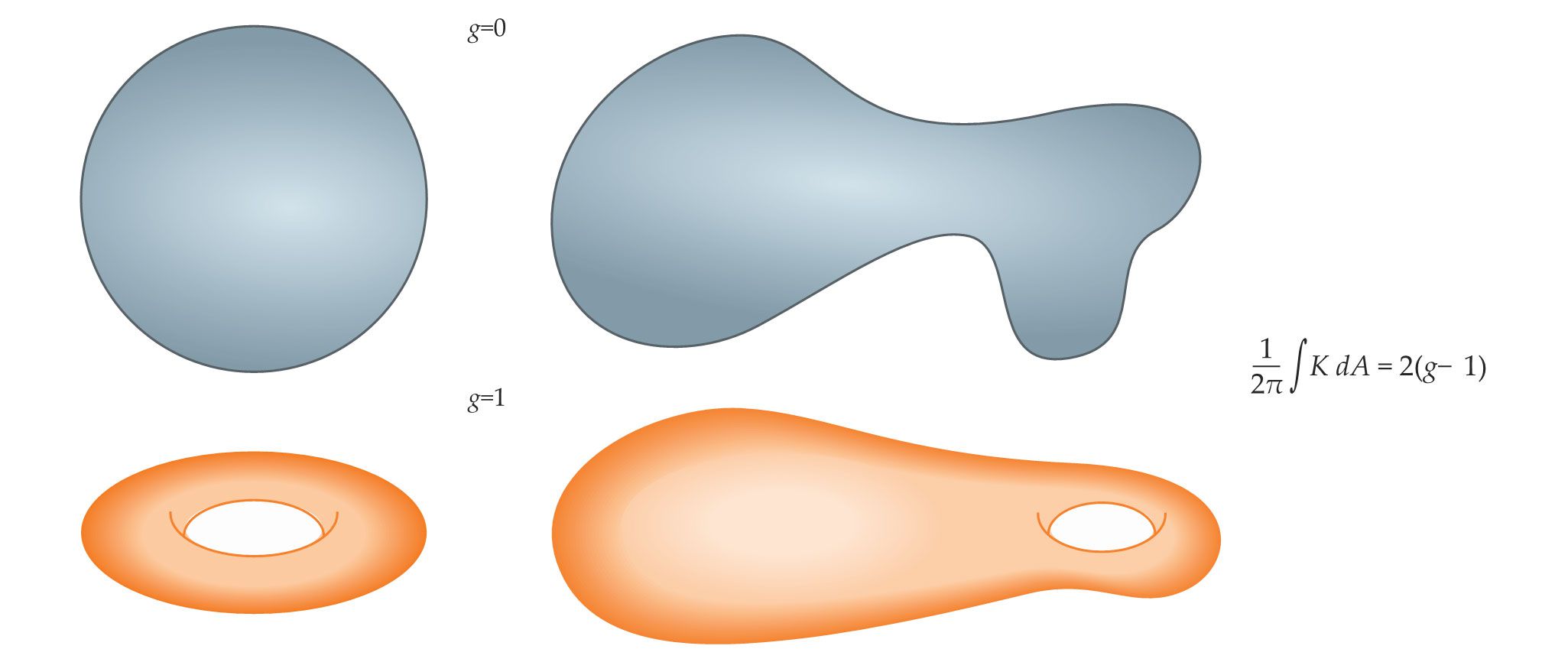
The notion of a topological invariant comes from the mathematical subfield of topology, which concerns those properties of geometric objects that are conserved under continuous deformations. The most famous such property is the genus
The remarkable implication of the Gauss–Bonnet theorem is that if one stretches the sphere so that some parts of the surface become more curved and other parts become flatter, the integer
Figure 1.

A topological invariant is a property of a geometric shape that does not change when the shape is stretched or distorted. One such invariant is the genus
Topological electrons
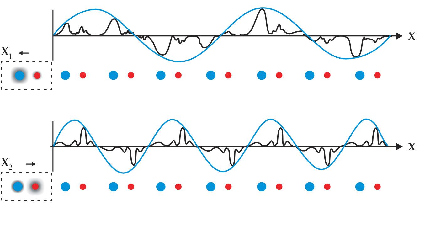
In an isolated atom, electrons occupy discrete quantum energy levels, or orbitals. But when many atoms are arranged in a crystal lattice, the electron wavefunctions from neighboring atoms hybridize with each other and the orbitals broaden into bands of states, each having a range of energies. A state in a band describes an electron that is shared among many atoms, and the electron’s wavefunction depends on the momentum
The electron momentum
In a discussion of an electron band’s topology, the Brillouin zone plays the role of a geometric space. Closed surfaces in the Brillouin zone can be likened to geometric shapes that have an integer-valued index akin to the genus. Importantly, the Brillouin zone has effective periodic boundary conditions: Exactly opposite points on the zone’s boundary are equivalent since they correspond to the same state with minimal de Broglie wavelength.
Constructing an analogue of the Gauss–Bonnet theorem for electron bands requires an analogue of curvature. As it turns out, that analogue arises from the properties of
Figure 2.

In a crystal, an electron state (black curve) is described by a slowly oscillating plane wave (blue curve) whose wavelength corresponds to the electron momentum that is modulated by a periodic Bloch function describing the electron’s attraction to the atoms (red and blue circles) in the crystal’s repeating unit cell. The electron probability density is shared among the atoms in the unit cell, as indicated by the shaded black areas in the outlined unit cells. The Berry connection
One caveat to the analogy with the Gauss–Bonnet theorem is that
Imagine now the hypothetical process of accelerating and then decelerating an electron such that the electron traces a path
The Berry phase becomes particularly instructive if we consider how it behaves for paths in a closed two-dimensional momentum space, such as the Brillouin zone of a 2D system, which is effectively closed because opposite edges of the zone are equivalent. Consider the green path shown in figure
Figure 3.

The Brillouin zone (
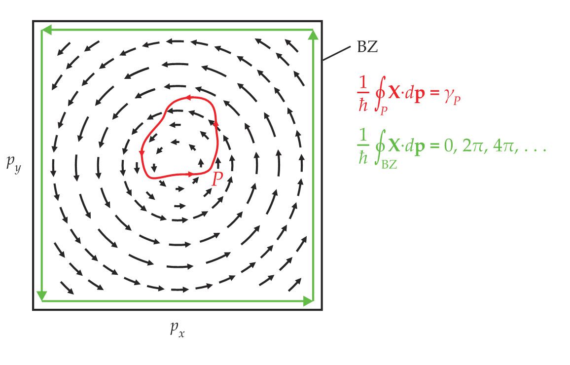
The condition on the Berry phase can be reformulated using Stokes’s theorem to change the contour integral along the Brillouin zone boundary into a surface integral across the entire Brillouin zone. That procedure gives
Having a nonzero Chern number requires symmetry breaking. In particular, in the Brillouin zone of a system with nonzero Chern number, the momenta
Implications of topology
As illustrated in figure
The analogy of Berry curvature to magnetic fields becomes clearer when one considers the effects of an applied electric field
One of the most striking implications of the magnetic field analogy arises from the motion of electrons at a sample’s boundary. If a conductor with no intrinsic Berry curvature is subjected to a magnetic field, electrons near the boundary perform skipping orbits—they essentially roll along the boundary in a direction defined by the magnetic field. The skipping orbits persist no matter how the boundary is shaped and provide a single conducting channel for current to flow through. In a 2D electron system with a magnetic field and sufficiently high electron mobility, the skipping orbits give rise to the celebrated quantum Hall effect, with a quantized electrical conductance whose value is universal. Similarly, the self-rotation implied by a nonzero Chern number guarantees the existence of traveling edge states. Two-dimensional materials with nonzero Chern numbers have the same universal conductance, even if no magnetic field is present.
The existence of a topological invariant for electron systems subjected to a magnetic field was first identified by David Thouless, Mahito Kohmoto, Peter Nightingale, and Marcel den Nijs and bears their initials (TKNN).
4
Their topological invariant accounts for a remarkable universality of the quantum Hall effect among different samples and materials (see the article by Joseph Avron, Daniel Osadchy, and Ruedi Seiler, Physics Today, August 2003, page 38 ). In fact, the TKNN invariant has allowed the universal constant
In quantum Hall systems, a magnetic field breaks time-reversal symmetry by forcing electrons to turn in spiral trajectories with a particular handedness set by the magnetic field direction. Playing those spiral trajectories backwards in time without reversing the sign of the external magnetic field produces motion inconsistent with the Lorentz force law. But edge states can exist in a topological material, even one that preserves time-reversal symmetry, if it combines broken inversion symmetry with a strong coupling between electron momentum and spin. (See the article by Xiao-Liang Qi and Shou-Cheng Zhang, Physics Today, January 2010, page 33 .) In the simplest case, those ingredients allow the two electron spin states to have nonzero but opposite Chern numbers.
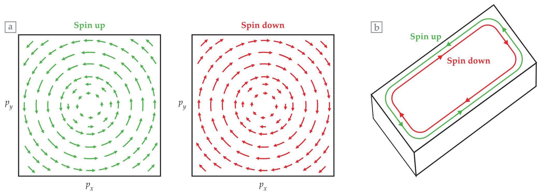
To see how that situation can arise, consider that under time reversal, a left-moving spin-up electron becomes right-moving and spin-down. Thus, a topological electron band can retain time-reversal symmetry if the bands for spin-up and spin-down electrons have opposite Chern number (figure
Figure 4.

A quantum spin Hall system has equal and opposite Chern numbers, which describe electron wavefunction winding, for its two spin species. (a) The Berry connection
Ultimately, the locking of spin and momentum in edge states arises from the microscopic spin–orbit coupling present in atomic orbitals. Spin–orbit coupling arises when a fast-moving electron experiences a magnetic field in its reference frame from the electrostatic potential of a nucleus. In the quantum spin Hall effect, strong spin–orbit coupling combines with broken inversion symmetry to produce a Berry curvature and a finite Chern number for each spin, even though no magnetic field is applied.
Topological bands in 3D
So far we have discussed only one example of a topological invariant: the Chern number in a 2D band that gives rise to edge states much like those in the quantum Hall effect. But 3D materials can also have electrical properties that are protected by a topological invariant. Those materials include topological insulators, which are usually narrow-bandgap semiconductors with strong spin–orbit coupling. 6 In topological insulators, an electrically insulating interior coexists with 2D metallic surface states in which electron spins are locked perpendicular to their momenta.
The 2D Chern number can also be applied to understand 3D Weyl semimetals. Such materials have special points in momentum space where their so-called topological charge is concentrated. To see why, imagine defining an arbitrary closed surface
Figure 5.

Berry curvature in a Weyl semimetal stems from monopole sources, known as Weyl points, where two electron bands meet in momentum space. (a) The Berry curvature
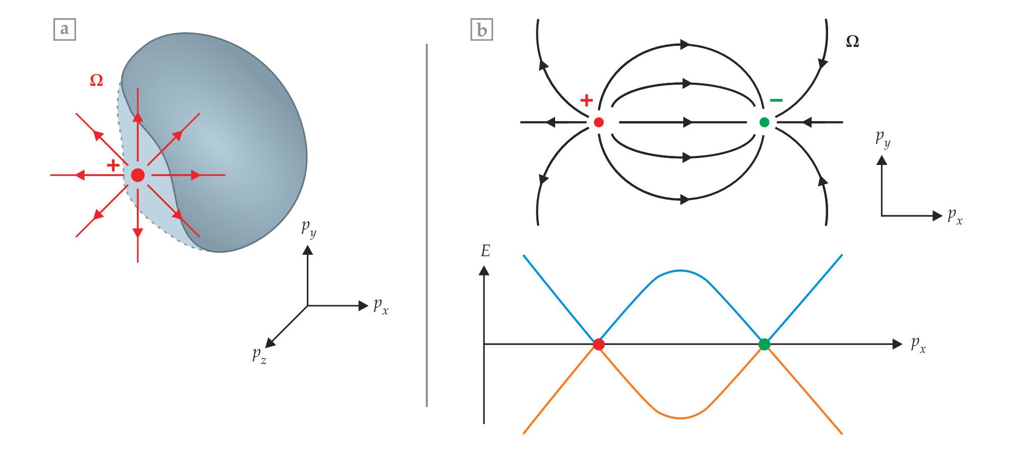
Given that
From a materials perspective, Weyl points arise when strong spin–orbit coupling causes two bands of electron states with different angular momentum to coincide in energy. The Weyl points correspond to the locations in momentum space where the two bands touch (see figure
In 1937, before the advent of modern topological band theory, Conyers Herring explained that two electron bands could meet—meaning they have the same energy—because of accidental degeneracies that prevent the two bands from hybridizing. 7 In that case, a perturbation that removes an accidental degeneracy can destroy the crossing and open a gap. In Weyl semimetals, however, the Weyl points are protected by the quantization of the Chern number. Only a sufficiently strong perturbation that brings two oppositely charged Weyl points together can destroy the degeneracy. Thus, Weyl semimetals are topologically protected gapless systems. Like other topological materials, they have intriguing surface states; in particular, their surfaces exhibit Fermi arcs, which are momentum states that connect the Weyl points. 8
Identifying and classifying topological materials remains a challenge. Materials are often grouped based on their band structures; that grouping works well for semiconductors whose energy gaps largely determine functionality. But topological materials are defined not only by their energy spectra but also by the symmetries of their electron wavefunctions. Topological quantum chemistry aims to capture that complexity in order to characterize materials based on both symmetry criteria and conventional band structures. 9 The computationally intensive endeavor has unexpectedly found that an estimated 27% of all materials are topological in nature. Searches have uncovered not only new topological materials, but entirely new classes of them, such as nodal-line semimetals 10 in which two bands touch along a line rather than a point in momentum space, and higher-order 3D topological insulators 11 whose edge states exist only as lines or points along the hinges or corners of the crystal.
The interplay between topological electrons and acoustic or magnetic excitations is also a burgeoning field of study. Topological concepts can even apply to phonons and magnons themselves, which suggests a vast terrain of new materials is waiting to be explored.
Experimentally, the study of topological materials is progressing rapidly. New compounds and even whole classes of topological materials are routinely being discovered. In 2008 M. Zahid Hasan and coworkers at Princeton University first observed 3D topological insulating behavior 12 using angle-resolved photoemission spectroscopy (ARPES) in Bi1−xSbx. Since then, many other topological insulators, Weyl semimetals, and nodal-line semimetals have been identified.
Technological prospects
Many materials derive their utility from their ability to either pass a current or prevent one from flowing. For example, the copper in a wire is useful because it allows electric current to flow freely, whereas the polymer encasing the wire stops the current from leaking out. Other materials pass or block heat currents, as do heat sinks on computer processors, or filter light, as do the frequency-selective lenses on protective sunglasses. From that perspective, the silicon age arose because semiconductors act as switchable valves for electrical current. We now know that pure silicon is a good insulator that only conducts if a gate voltage is applied to its surface.
New electronic materials usually have two performance targets: filtering and sensitivity. The material should be able to selectively pass or block a generalized current in much the same way as silicon selectively transmits electrical current. It should also exhibit a strong response to some input, like the way silicon p–n junctions turn light into electricity. Topological materials offer the promise of truly new technologies in those areas. They are interesting filters because their Berry curvature is a kind of handedness that breaks the symmetry between clockwise and counterclockwise motion. Topological materials can therefore act like doorknobs that open when turned in the correct direction but block motion in the wrong direction.
One striking application is in spin filtering. As illustrated in figure
Topological materials are unusually responsive to many kinds of applied fields because of their gapless, topologically protected electron bands. For example, the topological edge states associated with a nonzero Chern number could serve as dissipationless current-carrying channels. They have the potential to replace superconductors for some applications, and they may even function at room temperature.
More generally, the protection of low-energy states in topological materials can be exploited in ways that would give them an advantage over conventional materials in which low-energy states are often distorted by disorder. The protection of a material’s electron band structure can cause its electrons to exhibit enormous mobility, which results in each electron making an outsized contribution to a current being carried. 15 Weyl semimetals are extremely sensitive to light, which may lead to a new generation of photodetectors and night-vision goggles. 16 (See Physics Today, July 2020, page 18 .) Topological semimetals also exhibit an unprecedented thermoelectric effect, the ability to convert waste heat into useful electric power. 17 Additionally, topological electrons are unusually sensitive to magnetic fields. For example, in a magnetic field the quantum levels of the electron—its Landau levels—are widely spaced in energy, and applying a magnetic field along the current direction strongly reduces the material’s electrical resistance, a phenomenon known as the chiral anomaly. 18
Whether topological materials will revolutionize our current electronic technologies remains to be seen. But ideas from topology have clearly established themselves in materials physics, and they are here to stay. They have led to predictions and observations of new materials and phenomena. Who can tell whether they will come to define our current era?
References
1. See M. Riordan, L. Hoddeson, Crystal Fire: The Birth of the Information Age, W. W. Norton (1997).
2. L. D. Landau, Zh. Eksp. Teor. Fiz. 7, 19 (1937).
3. F. Bloch, Z. Phys. 52, 555 (1929). https://doi.org/10.1007/BF01339455
4. D. J. Thouless et al., Phys. Rev. Lett. 49, 405 (1982). https://doi.org/10.1103/PhysRevLett.49.405
5. K. von Klitzing, Phys. Rev. Lett. 122, 200001 (2019). https://doi.org/10.1103/PhysRevLett.122.200001
6. C. Kane, J. Moore, Phys. World 24(02), 32 (2011). https://doi.org/10.1088/2058-7058/24/02/36
7. C. Herring, Phys. Rev. 52, 365 (1937). https://doi.org/10.1103/PhysRev.52.365
8. X. Wan et al., Phys. Rev. B 83, 205101 (2011). https://doi.org/10.1103/PhysRevB.83.205101
9. B. Bradlyn et al., Nature 547, 298 (2017). https://doi.org/10.1038/nature23268
10. C. Fang et al., Chin. Phys. B 25, 117106 (2016). https://doi.org/10.1088/1674-1056/25/11/117106
11. F. Schindler et al., Sci. Adv. 4, eaat0346 (2018). https://doi.org/10.1126/sciadv.aat0346
12. D. Hsieh et al., Nature 452, 970 (2008). https://doi.org/10.1038/nature06843
13. I. Žutić, J. Fabian, S. Das Sarma, Rev. Mod. Phys. 76, 323 (2004). https://doi.org/10.1103/RevModPhys.76.323
14. K. F. Mak, D. Xiao, J. Shan, Nat. Photon. 12, 451 (2018). https://doi.org/10.1038/s41566-018-0204-6
15. T. Liang et al., Nat. Mater. 14, 280 (2015). https://doi.org/10.1038/nmat4143
16. C.-K. Chan et al., Phys. Rev. B 95, 041104(R) (2017). https://doi.org/10.1103/PhysRevB.95.041104
17. B. Skinner, L. Fu, Sci. Adv. 4, eaat2621 (2018). https://doi.org/10.1126/sciadv.aat2621
18. A. A. Burkov, J. Phys.: Condens. Matter 27, 113201 (2015). https://doi.org/10.1088/0953-8984/27/11/113201
More about the authors
Arthur Ramirez is a professor of physics at the University of California, Santa Cruz. Brian Skinner is an assistant professor of physics at the Ohio State University.


