Cryogenics on a Chip
DOI: 10.1063/1.1768673
How do you define the temperature of an electron gas? Like particles in general, electrons in a metal prefer to occupy energy levels in a way that minimizes their total energy. As fermions, they obey the Pauli exclusion principle and at zero temperature completely fill all the states below the Fermi energy. At nonzero temperatures, some electrons are found above the Fermi level by an amount k B T, the thermal energy of the system. More quantitatively, electrons at a particular temperature occupy energy levels with a probability given by the Fermi–Dirac distribution f(E) = 1/[1 + exp(E/k B T)]. Electrons reach this distribution by inelastic scattering—exchanging energy between themselves or with the surrounding crystal lattice.
Any probe that is sensitive to the width of the electron distribution function can work as a thermometer. By the same token, any device that narrows the electron distribution—by coupling the electron gas in one system to another that systematically removes hot electrons and replaces them with colder ones, for example—functions as a refrigerator. Advances in micro- and nanotechnologies are increasingly allowing researchers to create such refrigerators using purely electrical means and to investigate a wide variety of nonequilibrium electron gas distributions.
In this article, we focus on a few novel devices that exploit the interplay between electrical and thermal properties to control temperatures by manipulating electrons in various conductors. The basic building block in many of these devices is a tunnel junction that connects and transports charge between two conductors. A tunnel junction is typically a very thin (roughly 1 nm) insulating layer between two metals, but it may also be a Schottky barrier between a semiconductor and a metal or a vacuum gap between conductors. Under the right conditions, a mere voltage source is enough to generate a nonequilibrium distribution of electrons.
Energy distributions in a wire
The simplest case of a nonequilibrium distribution occurs in a different kind of weak link, namely a narrow wire that connects two metallic reservoirs, as shown in figure 1. Electrons in the bulky reservoirs at both ends follow Fermi–Dirac statistics. That is, their energy distribution is thermal, but with electron energies shifted by an amount eU, the difference in the chemical potential between them, induced by an applied bias voltage U. The far left and far right panels of figure

Figure 1. A gold wire in this micrograph connects two metallic reservoirs that form a circuit. (a) A bias voltage U shifts the energy distribution f(E) of electrons in the left reservoir relative to the distribution in the right. The energy distribution in the wire (center panel) is complicated: As measured by the probe finger pictured in the micrograph, f(E) depends on whether the electrons reach thermal equilibrium with the lattice more quickly than they diffuse through the wire (blue), whether their energy equilibrates slowly with lattice phonons (red), or whether they diffuse through the wire more quickly than electrons can equilibrate with each other and the surrounding lattice phonons (green). (b) Experimental curves illustrate the effect of different bias voltages on the structure and width of the electron distribution.
(Adapted from ref. 2)
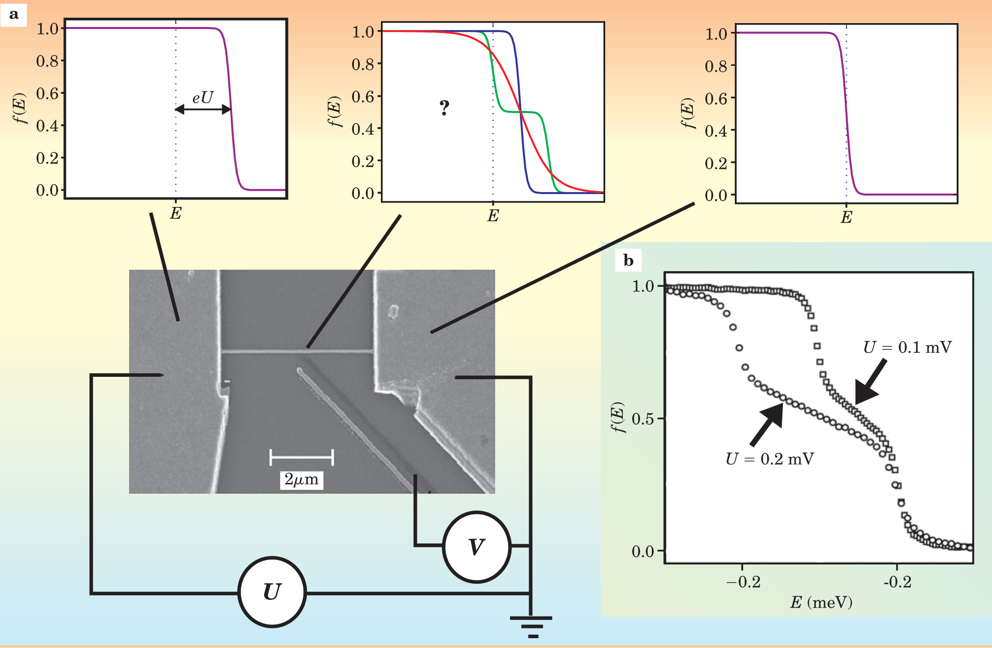
If the electron–phonon relaxation is slow but the electron–electron relaxation is faster than the transit time, then one can still assign a temperature to each section of the wire. Electrons will be heated above the lattice temperature, and the resulting electron temperature varies with position and reaches its highest value in the center of the wire. The more broadly curved energy distribution (in red) illustrates that hot-electron regime. Note that the size of the applied voltage, rather than the temperature of the chip, predominantly controls the width of the distribution.
The most interesting regime, however, is when the wire is short and made of pure enough material to reduce the diffusion time of electrons well below even the electron–electron relaxation time. In that regime, one cannot meaningfully assign any temperature to the wire, even though the reservoirs remain fixed at their original temperatures. The energy distribution in the wire strongly deviates from the Fermi–Dirac distribution and resembles instead a position-dependent superposition of the different distributions in the reservoirs. The result is a double steplike structure; in the middle of the wire, half of the electrons equilibrate to the temperature in the left reservoir and half equilibrate to the temperature in the right.
Hugues Pothier and his colleagues first observed the actual two-step distribution in 1997. 1 Relaxation rates affected the detailed shape of the distribution they observed 2 and the experiments produced interesting results on the nature of electron–electron interactions in nanostructures. Jochem Baselmans and collaborators from the University of Groningen exploited similar nonequilibrium distributions in a wire to control the critical current drawn through a superconductor–normal metal–superconductor (SNS) weak link. 3 In what follows, we are going to see how one can narrow the energy distributions—that is, how one can cool the electron gas—instead of broadening the distribution (heating) or distorting its shape.
NIS junctions
Normal-metal–insulator–superconductor (NIS) tunnel junctions form the simple building blocks used in many devices because they are capable of both measuring and manipulating electronic distributions. Consider figure 2, which depicts an energy-level diagram of a NIS junction biased at a voltage just slightly below Δ/e, where Δ is the energy gap of the superconductor and e the charge on an electron. Electrons can be transported through the junction only by elastic tunneling, crossing the insulating barrier horizontally as shown. Because eV and k B T are typically many orders of magnitude smaller than the Fermi energy E F, we are only interested in energies very close to the Fermi level. Therefore, the density of states in the normal metal is nearly constant, and electrons normally occupy those states in a way that follows the Fermi–Dirac distribution.

Figure 2. Normal-metal–insulator–superconductor (NIS) tunnel junctions as electron thermometers and refrigerators. (a) In this energy-level diagram of a NIS tunnel junction, the energy gap around the superconductor’s Fermi level forbids electrons from tunneling between the normal metal and the superconductor at the energy levels shown. A bias voltage V across the junction separates the chemical potentials by eV. (b) A hybrid electronic cooler is formed from two NIS junctions connected in series: The central part is a copper island, coupled to NIS probing junctions and large NIS injection junctions. The thermometer’s voltage V TH is measured across the NIS probing junctions in a circuit biased at constant current; the control voltage V C is applied across the injection junctions. (c) The current–voltage (I–V) curves indicate the monotonic decrease in voltage as the temperature rises in such a device biased at constant current I 0—an effect that makes the device a thermometer. (d) Experimental curves show the cooling response at various bath temperatures (600, 400, 340, and 290 mK). Applying a nonzero V C reduces the temperature as hot electrons evaporate away. The copper island’s minimum temperature occurs when eV C ≃ 2Δ (the factor of 2 occurs because the two junctions are configured in series).
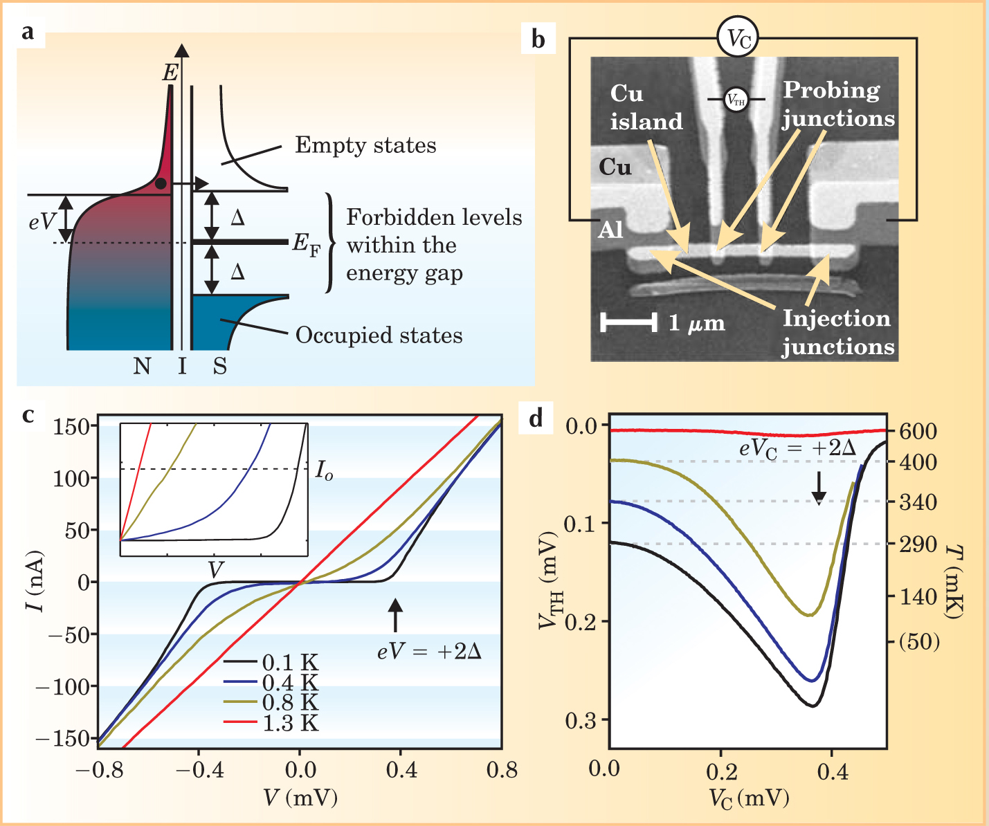
The energy gap of the superconductor, with forbidden states within ±Δ of the Fermi level, is what makes this system so significant. Provided temperatures remain well below the critical temperature of the superconductor, the states just below that gap are almost completely filled and those above it almost completely empty. This condition sets the stage for the charge and heat transport that can occur in NIS devices. Voltages below Δ/e prohibit any current because no available states exist in the superconductor to accommodate electron tunneling. Above the gap voltage, current increases rapidly. As the temperature rises, the electron distribution broadens in the normal electrode, and the threshold voltage for current flow becomes increasingly blurred.
Whether used at constant voltage or constant current, NIS devices are therefore sensitive low-temperature thermometers. While Daniel Schmidt was a postdoc at the University of California, Santa Barbara, he and coworkers developed a fast NIS thermometer that operates at submicrosecond timescales, for instance. 4 As shown by Pothier and colleagues, NIS structures can also be used to map out nonequilibrium electron distributions. Two separate threshold voltages for current onset were observed in their experiment. This produced the double-step distribution measured in figure 1.
In addition to serving as a thermometer, NIS junctions are also the basic elements in one of the few thermoelectric refrigerators that has been proven experimentally to work. 5–8 As shown in figure 2, when the junction is biased close to the gap voltage, only electrons occupying states above the Fermi energy in the normal metal can tunnel through the barrier. The removal of those hot electrons cools the metal electrode in a manner analogous to cooling a cup of coffee by evaporation. To maintain charge balance, the lost electrons must be replaced in the metal. Either a metal–superconductor contact—excluding the tunnel barrier—or more commonly, a second NIS contact can be used to add cold electrons. If the electron–electron interaction rate in the normal metal exceeds the tunneling rate, then the metal’s electrons occupy a Fermi–Dirac distribution with a lower temperature than the lattice. In the opposite limit, a nonequilibrium electronic distribution forms.7, 9 Typically, the refrigerator reaches its base temperature when the cooling power of the junctions matches the heat leaking from lattice phonons to electrons in the metal. Existing submicron NIS refrigerators can cool electrons from 300 mK down to below 100 mK, 6,7 although the cooling powers are typically only fractions of a picowatt.
Thermometers on a chip
Virtually any quantity that varies with temperature can be used as a thermometer. But its particular characteristics determine whether a thermometer is suitable for a particular application. Ideal thermometers cover a wide temperature range, follow a simple and monotonic temperature dependence, exhibit little self-heating, and respond quickly to temperature change. Other desirable characteristics include easy operation, small size and thermal mass, and immunity to external phenomena such as magnetic fields. (For reviews on low-temperature thermometry, see reference 10 and the article by Robert Soulen and William Fogle in Physics Today, August 1997, page 36 .)
Because they are so sensitive to magnetic fields, hybrid metal–superconductor devices are not ideal for general purpose thermometry. Tunnel junctions between normal metals (NIN) solve that problem—the I–V curves in devices made of these materials are insensitive to magnetic fields. But they also happen to be temperature independent to first approximation. Surprisingly, then, Coulomb blockade (CB) and shot-noise thermometers—perhaps the most interesting on-chip thermometers—are both NIN structures. These devices also belong to the rare category of primary thermometers—that is, they measure absolute temperatures without the need to calibrate against other thermometers or fixed points.
Coulomb blockade thermometry
Any physics student knows that the energy of a capacitor depends on the charge Q as Q 2/2C, where C is the capacitance. In macroscopic systems—say, ordinary capacitors on a circuit board at ambient temperatures—charge can be treated as a continuous variable. That is, in those systems, the spatial charge distribution behaves as if the polarization can change continuously. And changes in the energy associated with the charge of a single electron are simply much smaller than k B T. But fundamentally, charge is quantized in units of the elementary charge, e, of an electron.
The microscopic nature of the tunnel junction exploits that property. It can be viewed as a capacitor, formed by the parallel-plate geometry of two conducting banks separated by a thin insulating barrier, in parallel with an “ideal” tunneling element. And a tunnel junction’s capacitance can be made tiny—typically femtofarads for a junction with linear dimensions well below 1 µm—using micro-and nanolithographic techniques. When connected in series, tunnel junctions form a so-called Coulomb island with femtofarad capacitances. That is more than three orders of magnitude smaller than the smallest capacitors on a circuit board or stray capacitances in macroscopic wiring. Charge quantization requires that an electron have an energy at least e 2/2C above the Fermi level in order to hop onto the island, a restriction that forms the basis for the CB effect.
When the temperature is low enough— k BT ≪ e 2/2C (the charging energy, E C)—well below 1 K for a femtofarad capacitor, no current can flow without a substantial bias voltage |V| > E C /e to inject and extract charges through the island. 11 In this low-temperature regime, tunnel junctions exhibit little temperature dependence.
However, at somewhat higher temperatures—the so-called partial CB regime—when k B T ≥ E C, the I–V characteristics of the tunnel junctions exhibit a pronounced temperature dependence (see figure 3). One of us (Pekola) and colleagues from the University of Jyväskylä in Finland discovered the effect in 1994 and developed a device, the Coulomb blockade thermometer, that exploits the interplay between the thermal and charging energies. 12,13 The graph in figure 3 illustrates the basic measurement on a CBT: the differential conductance versus bias voltage V across a sensor that consists of many parallel linear arrays of islands connected by junctions. The differential conductance is the slope of the I–V curve, normalized to its asymptotic value. The weak CB effect at operating temperatures creates a drop in the conductance at low values of the voltage.

Figure 3. (a) This micrograph shows part of a typical Coulomb blockade thermometer (CBT) array, with adjacent junctions separated by 8 µm. (b) At very low temperature (black), there exists an abrupt voltage offset in the I–V curve around zero bias through a Coulomb blockade island. At high temperature (red), for which the thermal energy is much larger than the elementary charging energy E C = e 2/2C, with C the island’s capacitance, the I–V curve is linear—or ohmic—and the Coulomb effect negligible. The CBT operates between these extremes in the so-called partial Coulomb blockade regime. In that regime (blue and green), the voltage offset is smeared in a predictable way determined by thermal fluctuations in the number of electrons on each island. (c) An experimental CBT conductance curve—the slope of the I–V curve versus voltage—has a characteristic temperature dependence in the partial Coulomb blockade region: eV 1/2 = 5.439Nk B T, where N is the number of junctions in the device.
(Micrograph courtesy of Juha Kauppinen, Nanoway Ltd.)
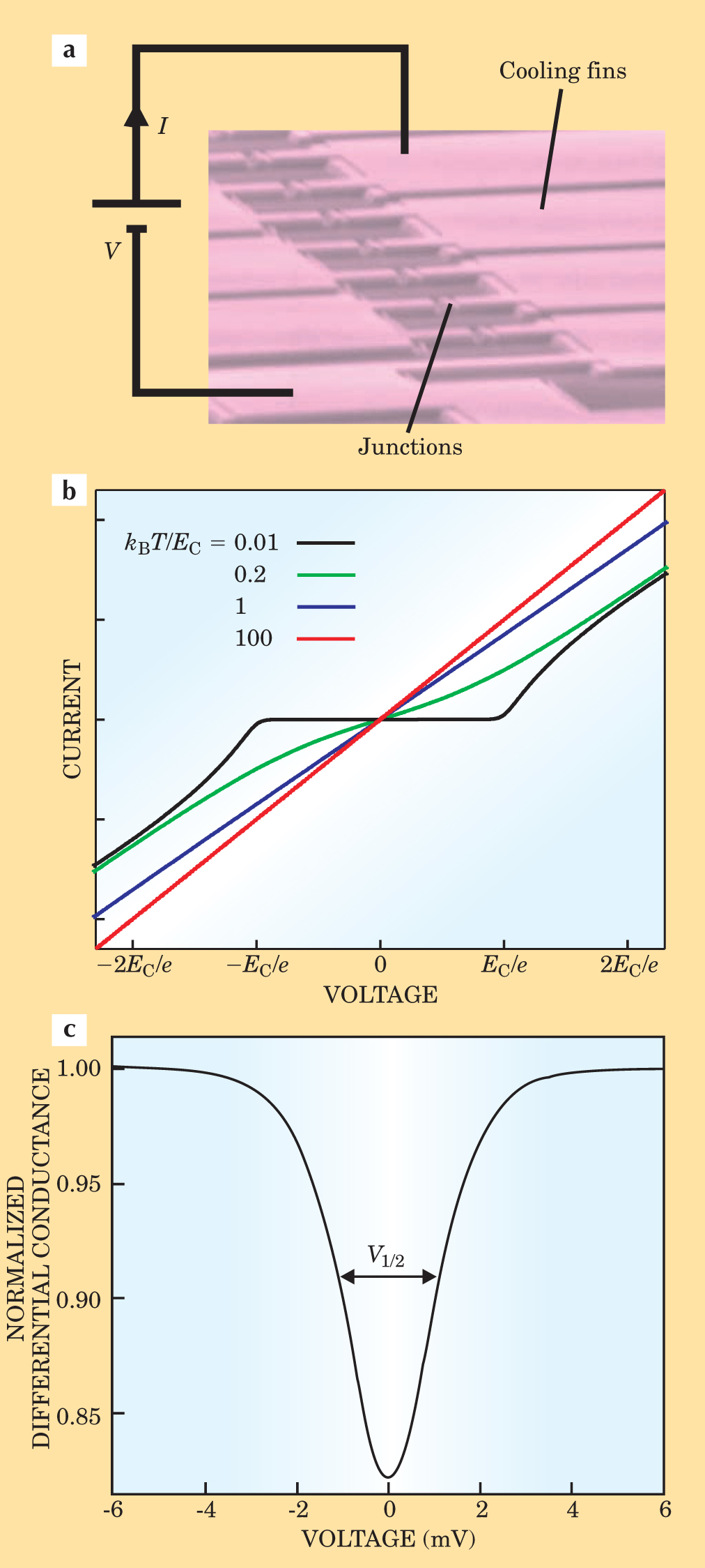
Remarkably, the conductance curve has a universal form. The full width at half minimum of the dip, indicated by V 1/2, depends only on temperature, Boltzmann’s constant, the electron charge, and the number N of junctions in series. In the “high” temperature limit, eV 1/2 = 5.439Nk B T. The depth of the dip, in figure
As a result, sensors suitable for different temperature regimes can be tailored by choosing the size of the junctions. The CBT’s operating temperatures range from about 20 mK up to above 30 K. Moreover, the thermometer’s absolute accuracy is better than 1% over two decades in temperature, even in high magnetic fields. The lowest lattice temperature accurately measurable by CBT can hardly be pushed much below 10 mK, though, because of rapid decoupling between electrons and phonons as temperature decreases.
Shot-noise thermometry
In both the NIS and CB thermometers, the current–voltage characteristics of the devices make them temperature sensitive. But another physical quantity, electrical noise—the fluctuations of current within a circuit—can depend on the electron distribution and thus the temperature in an even simpler device and over a wider temperature range. At Yale University, Lafe Spietz, one of us (Schoelkopf), and coworkers have demonstrated that by measuring the electrical noise of an NIN tunnel junction, an accurate primary thermometer can be created that operates between room temperature and the millikelvin range using a single sensor. 14 To appreciate how this shot-noise thermometer (SNT) works, consider again the picture of electron transport in tunnel junctions, but modified to include the fluctuations in the current induced by a finite temperature and bias voltage (see figure 4). A single, relatively large NIN junction has no CB effect, and the density of states for electrons in the metals is roughly constant. So the conduction is ohmic for all voltage biases and temperatures that are small compared to the Fermi energy.

Figure 4. The shot-noise thermometer, pictured in (a), consists of a tunnel junction and amplification electronics. One set of leads current biases the junction while the other lets one measure the average DC voltage across the junction. The circuit amplifies the current noise in a wide bandwidth and measures the total power as a function of the applied voltage. (b) The noise power measured as a function of normalized voltage (x = eV/k B T) across the junction at two different temperatures follows a simple theoretical form, P ~ x/2 coth(x/2). Shot noise (blue dashes) and Johnson noise (green dashes) are the limits of that expression. (c) At equilibrium (V = 0), bottom, the Fermi levels line up and the net current is zero. But as the thermal width of the electron distributions increases, so does the noise; that is the well-known Johnson noise. At high bias (eV ≫ k B T), top, the electron distribution function is offset by more than its thermal width. In that regime, the current and shot noise both increase linearly with V. The two limits of the noise power versus voltage curve thus convert the temperature into a measured bias voltage using only k B and e.
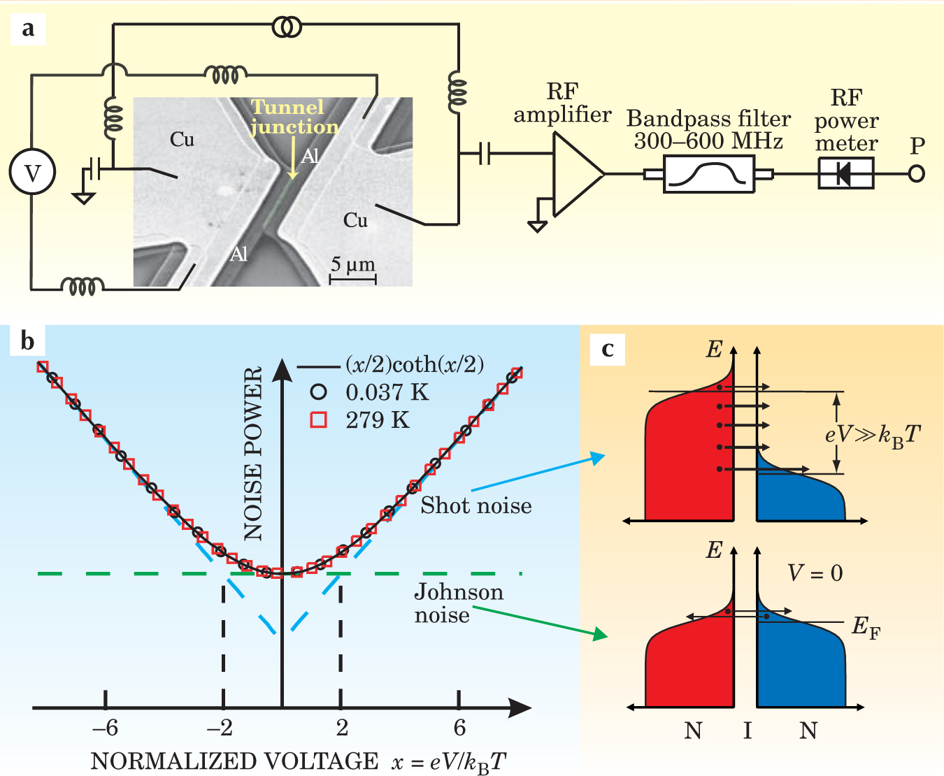
At zero bias voltage, there is obviously no average current. However, at nonzero temperatures, the smearing of the electron distribution functions (see figure
In a junction with bias voltages large enough that eV ≫ k B T, the offset in the chemical potentials of the two metals means that there are many filled states on one side that can tunnel into empty states on the other side, and a net current flows, as shown in figure
Spietz and collaborators showed that such a thermometer could operate over four orders of magnitude in temperature—from 300 K to 30 mK—with accuracies of better than 0.1% in the middle two decades of that range. Because the conversion factor in the SNT, and in the CBT thermometer described previously, involves only the fundamental constants e and k B, both are primary thermometers. One can therefore imagine future implementations that might lead to a new quantum standard of temperature that would follow the successful redefinitions of the volt and the ohm in terms of Josephson and quantum Hall effects in solid-state devices.
Applications of microthermometry
The SNT promises high accuracy, but the general nature of noise measurements tends to make it a slower and somewhat less sensitive thermometer. Other research has developed microthermometers with high sensitivity or speed to study basic physics or as detectors in astrophysical applications. Tunnel junctions are used in superconducting quantum interference devices (SQUIDs), for instance, to make current amplifiers of remarkable sensitivity that can make traditional Johnson noise thermometry vastly more sensitive. 15 While at Caltech, Keith Schwab and coworkers used such techniques to study the thermal conductivity of freestanding nanomachined structures 16 and to observe the quantization of thermal conductance. Future generations of this type of device may even detect single phonons.
The transition-edge sensor, another highly sensitive microthermometer, relies on the rapid change in the resistance of a superconducting thin film at its transition temperature. These devices typically operate between 0.1 and 4 K, a temperature range in which thermal noise is low. (See the article by Caroline Stahle, Dan McCammon, and Kent Irwin in Physics Today, August 1999, page 32 .) Again, it is only the electrons within a micron- to millimeter-sized lithographic structure whose temperature is sensed. Careful design has produced hot-electron mixers consisting of small transition-biased links whose temperature can respond to incident power on time scales of only a few tens of picoseconds, fast enough to make wide-bandwidth heterodyne detectors for terahertz radiation. 17
Transition-edge sensor thermometers also form the heart of microcalorimeters and microbolometers that are now finding application in fields as diverse as astrophysics and terrestrial materials analysis. These devices detect the energy deposited by individual optical and x-ray photons, or the power deposited by a flux of longer wavelength photons. A sensor consists of a thermally isolated absorber and a transition-edge thermometer whose output signal is measured with a cryogenic SQUID amplifier. Researchers are making rapid progress in fabricating and deploying large arrays of these sensors. Based on this technology, they are developing a new generation of astronomical instruments that will measure the spectrum from x-ray to millimeter wavelengths. These instruments are intended to address fundamental cosmological questions such as the extent of polarization in the microwave background.
Future work
What will the future of this research hold? At the moment, cryogenic detector systems use temperatures below 1 K to achieve their high sensitivity and rely on conventional cooling techniques such as adiabatic demagnetization or helium dilution refrigerators. However, those refrigeration techniques can be cumbersome on the production floor of a factory or in a spacecraft used for astronomical research. Because only small amounts of heat need to be removed from the tiny heart of these chips to cool them, the hope is to integrate the detectors with a NIS cooler or some similar mi-crorefrigerator that forms a complete low-temperature apparatus on a chip. Scientists at NIST in Boulder, Colorado, are pursuing that goal, striving to build laboratory instruments based on the manipulation of electron gases.
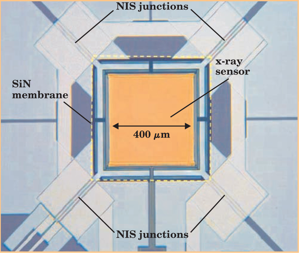
Together with researchers from the University of Notre Dame and the European Space Agency, one of us (Ullom) and colleagues from NIST have successfully scaled the tunnel junction refrigerators described in this article to much larger sizes. 8 The refrigerators have larger cooling powers and can be made using conventional photolithographic fabrication techniques. The NIST team is now making devices in which tunnel junction refrigerators cool other cryogenic electronics, such as transition-edge photon sensors. At such low temperatures, the sensors will be able to resolve x-ray energies with a precision of about one part in 1000. Figure 5 shows a prototype device that combines an x-ray sensor with a tunnel junction refrigerator. One goal of the work is to build a simple cryogenic spectrometer to measure x-ray fluorescence on a scanning electron microscope without requiring the complicated cryogenic apparatus usually necessary for creating millikelvin temperatures.

Figure 5. This micrograph shows an integrated x-ray sensor and refrigerator. The sensor is made of a thin bilayer of molybdenum and copper and has a superconducting transition temperature near 100 mK. The electrical resistance of the sensor changes when it absorbs an x ray. Two normal-metal–insulator–superconductor tunnel junctions sit at each corner of a silicon nitride membrane that supports the sensor. The junctions cool “Y”-shaped cold fingers that extend onto the membrane and act as heat sinks for the sensor.
It is now well known that quantum-effect devices and nanostructures can have novel electrical properties that allow physicists to control and measure charges or even spins in unprecedented ways. In the near term, such developments should lead to new measurement capabilities and new physics; in the longer term, to new kinds of circuits and technologies. In this article, we have dicussed some of the ways in which tiny devices can also be used to measure and control thermal properties on small scales. Recent work has produced a number of useful devices, although most operate only at cryogenic or subkelvin temperatures. The more ambitious goal is the construction of an on-chip refrigerator that could span the large range between ambient and millikelvin temperatures using purely electrical means. Achieving that goal might banish altogether the need for traditional cryogenics.
References
1. H. Pothier, S. Guéron, N. O. Birge, D. Esteve, M. H. Devoret, Phys. Rev. Lett. 79, 3490 (1997).https://doi.org/10.1103/PhysRevLett.79.3490
2. A. Anthore, “Decoherence Mechanisms in Mesoscopic Conductors,” PhD thesis, U. of Paris VI (2003).
3. J. J. A. Baselmans, A. F. Morpurgo, B. J. van Wees, T. M. Klapwijk, Nature 397, 43 (1999).https://doi.org/10.1038/16204
4. D. R. Schmidt, C. S. Yung, A. N. Cleland, Appl. Phys. Lett. 83, 1002 (2003).https://doi.org/10.1063/1.1597983
5. M. Nahum, T. M. Eiles, J. M. Martinis, Appl. Phys. Lett. 65, 3123 (1994).https://doi.org/10.1063/1.112456
6. M. M. Leivo, J. P. Pekola, D. V. Averin, Appl. Phys. Lett. 68, 1996 (1996);https://doi.org/10.1063/1.115651
M. A. Tarasov, L. S. Kuz’min, M. Yu. Fominskii, I. E. Agulo, A. S. Kalabukhov, J. Exp. Theor. Phys. Lett. 78, 714 (2003).https://doi.org/10.1134/1.16482937. J. P. Pekola, T. T. Heikkilä, A. M. Savin, J. T. Flyktman, F. Giazotto, F. W. J. Hekking, Phys. Rev. Lett. 92, 056804 (2004).https://doi.org/10.1103/PhysRevLett.92.056804
8. A. M. Clark, A. Williams, S. T. Ruggiero, M. L. van den Berg, J. N. Ullom, Appl. Phys. Lett. 84, 625 (2004).https://doi.org/10.1063/1.1644326
9. W. M. van Huffelen, T. M. Klapwijk, D. R. Heslinga, M. J. de Boer, N. van der Post, Phys. Rev. B 47, 5170 (1993).https://doi.org/10.1103/PhysRevB.47.5170
10. O. V. Lounasmaa, Experimental Principles and Methods Below 1 K, Academic Press, New York (1974);
F. Pobell, Matter and Methods at Low Temperatures, 2nd ed., Springer-Verlag, New York (1996).11. For a review of Coulomb blockade and single-electron tunneling phenomena, see D. V. Averin, K. K. Likharev, in B. L. Altshuler, P. A. Lee, R. A. Webb (eds.), Mesoscopic Phenomena in Solids, Elsevier Science, New York (1991), p. 173.https://doi.org/10.1016/B978-0-444-88454-1.50012-7
12. J. P. Pekola, K. P. Hirvi, J. P. Kauppinen, M. A. Paalanen, Phys. Rev. Lett. 73, 2903 (1994);https://doi.org/10.1103/PhysRevLett.73.2903
M. Meschke, J. P. Pekola, F. Gay, R. E. Rapp, H. Godfrin, J. Low Temp. Phys. 134, 1119 (2004).https://doi.org/10.1023/B:JOLT.0000016733.75220.5d13. T. Bergsten, T. Claeson, P. Delsing, Appl. Phys. Lett. 78, 1264 (2001).https://doi.org/10.1063/1.1351526
14. L. Spietz, K. W. Lehnert, I. Siddiqi, R. J. Schoelkopf, Science 300, 1929 (2003).https://doi.org/10.1126/science.1084647
15. C. P. Lusher, J. Li, V. A. Maidanov, M. E. Digby, H. Dyball, A. Casey, J. Nyeki, V. V. Dmitriev, B. P. Cowan, J. Saunders, Meas. Sci. Technol. 12, 1 (2001).https://doi.org/10.1088/0957-0233/12/1/301
16. K. Schwab, E. A. Henriksen, J. M. Worlock, M. L. Roukes, Nature 404, 974 (2000).https://doi.org/10.1038/35010065
17. A. D. Semenov, G. N. Gol’tsman, R. Sobolewski, Supercond. Sci. Technol. 15, R1 (2002).https://doi.org/10.1088/0953-2048/15/4/201
More about the authors
Jukka Pekola is a professor in the Low Temperature Laboratory at Helsinki University of Technology, in Finland.
Robert Schoelkopf is a professor in the departments of applied physics and physics at Yale University in New Haven, Connecticut, and Joel Ullom is a staff physicist at the National Institute of Standards and Technology in Boulder, Colorado.
Jukka Pekola, 1 Low Temperature Laboratory, Helsinki University of Technology, Finland .
Robert Schoelkopf, 2 Yale University, New Haven, US .
Joel Ullom, 3 National Institute of Standards and Technology, Boulder, Colorado, US .


