ASM International’s innovative divisions
DOI: 10.1063/PT.3.4857

Increased specialization has been the name of the game in the semiconductor industry since its birth in 1947. The $439 billion business is made up of firms of all stripes. 1 Some design and manufacture chips in-house. Others specialize in manufacturing or design. Still others fabricate parts of chips. Then there are equipment manufacturers, material suppliers, and component subcontractors—and research centers that drive innovation.

ISTOCK.COM/LEMONO
The industry’s specialization is an example of a bedrock principle of economics: the division of labor, or the separation of work into its component tasks. Perhaps best exemplified by the late-19th-century assembly line, it was first described by Adam Smith in his 1776 treatise The Wealth of Nations, which outlined how the division of labor improves workers’ skills, saves time, and enables further technological advancement. In the case of the semiconductor industry, it accelerated the development of more advanced chips, which in turn enabled new applications, increased growth, and stimulated further specialization that kept expanding as the semiconductor industry grew. 2
The history of ASM International, one of the industry’s juggernauts, serves as an illustrative lens for understanding specialization. Founded in 1964 by Dutch entrepreneur Arthur del Prado (1931–2016) as Advanced Semiconductor Materials, ASM is a global leader in the production of semiconductor manufacturing equipment. Under Del Prado, who retired in 2008, ASM pioneered manufacturing techniques, such as atomic layer deposition, and successfully brought them to market. The company, which Del Prado registered as private in 1968, casts a large shadow over the industry: Three other major semiconductor companies, ASML, Besi, and ASM Pacific Technology, originally started as divisions of ASM.
Del Prado’s beginnings
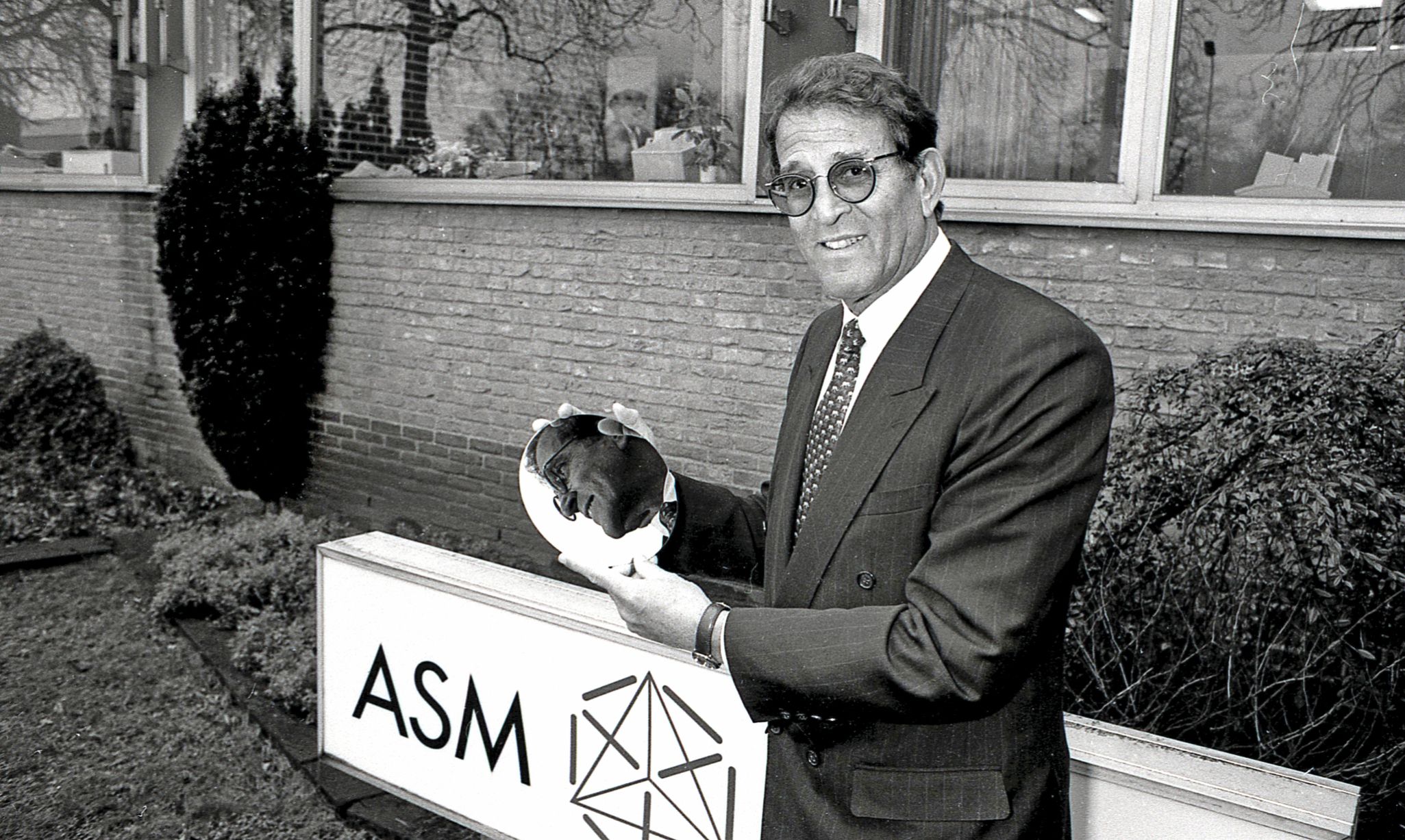
ASM’s history is closely tied to Del Prado, seen in figure
Figure 1.

Arthur del Prado holds a silicon wafer in front of ASM International’s headquarters in Bilthoven, the Netherlands, in 1996. Del Prado founded ASM in 1964 and was its CEO until 2008. (Photo by Fotopersbureau Dijkstra.)
Born in what is now Jakarta, Indonesia, Del Prado had a tumultuous early life. During World War II, he was detained in a prison camp on the island of Java when the Japanese occupied what was then the Dutch East Indies. Raised in the Netherlands after the war, he moved to the US in 1954 after graduating from college. He ended up in the San Francisco Bay Area, where in 1957 he bumped into engineer Dean Knapic, who had recently established a new venture called Knapic Electro-Physics (KEP).
Knapic had formerly worked with semiconductor innovator William Shockley at Shockley Semiconductor Laboratory. He left that firm as an expert in the Czochralski method, one of the most effective techniques to create monocrystalline silicon.
3
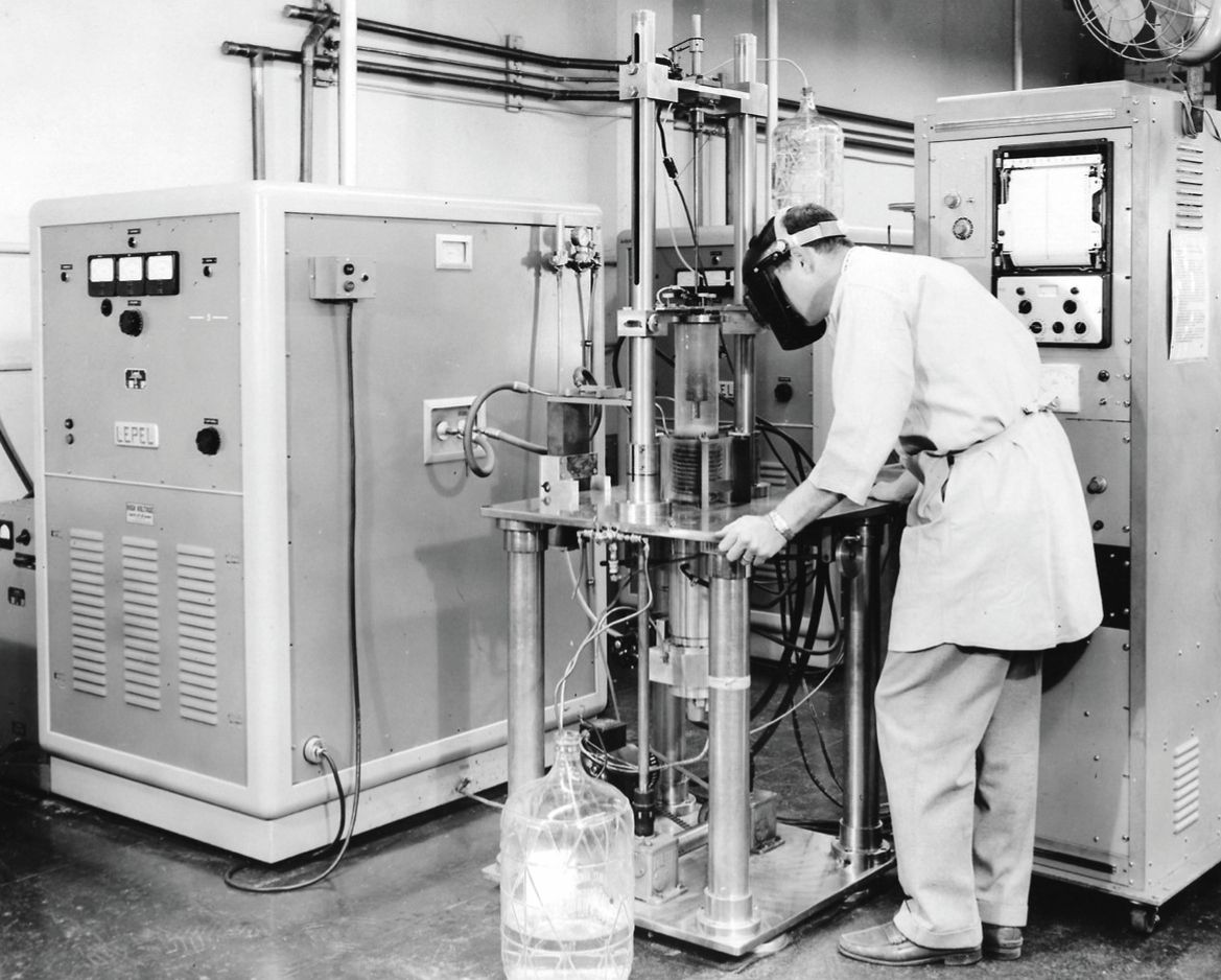
It involves mounting a thin seed of silicon on a rod, dipping it in molten polysilicon, and then withdrawing the rod while slowly rotating it. That process creates a monocrystalline silicon shaft (see figure
Figure 2.

Knapic Electro-Physics was one of the first companies to sell silicon crystals. It produced them using the Czochralski method, which required machinery like the crystal puller pictured here. (Courtesy of the Arthur del Prado Collection.)
That proved to be the turning point in Del Prado’s career. When he returned to the Netherlands in 1958, Del Prado spearheaded the development of the European market for silicon crystals. In those days international calls were still extremely expensive, which meant that he was able to communicate with KEP headquarters in Palo Alto, California, via only airmail and telegrams. Because of the geographic separation, Del Prado built trust with the company through his sales. He wrote to businesses across Europe and built a customer base that spanned the continent. Most of his clients were semiconductor manufacturers whose names are long lost in memory. Customer satisfaction was critical to Del Prado, who never gave no for an answer, even if he was unsure if KEP could fulfill the clients’ demands. His sales increased from $9000 in 1958 to $249 300 in the first nine months of 1960. By 1963 Del Prado served 40% of the European silicon market.
But KEP did not last long. It faced increasing competition in the silicon crystals market in the early 1960s. Silicon was rapidly becoming the standard material from which semiconductors were made, and more semiconductor manufacturers began producing silicon crystals internally. Another manufacturing technique called float-zone refining also began gaining popularity. That method involved slowly melting a polysilicon rod and allowing it to crystallize into monocrystals. Even though the Czochralski method would again become predominant when the size of silicon wafers increased, at that time float-zone refining was more economical because it enabled manufacturers to control for silicon impurities more easily.
KEP also faced increasing demand for silicon wafers coated with an epitaxial film of silicon. Such a film offered more control over the material’s conductive and crystalline properties. But Knapic refused to pursue any of those innovative techniques and insisted that KEP stick to the Czochralski method. As a result, the company’s sales declined in the early 1960s. Investors attempted to revive KEP’s fortunes by sidelining Knapic and installing new management, but that proved fruitless. KEP closed in early 1964.
Del Prado was now a free agent, and he quickly founded a new company called Advanced Semiconductor Materials—now ASM International. He drew two major conclusions from KEP’s demise. First was that a founder could lose control of their company if it had external investors. Having been responsible for his own success so far, Del Prado was determined to secure maximum elbow room for himself. He would not face Knapic’s fate. The second was that it was crucial for a business like KEP to diversify its operations. The rise of float-zone-grown silicon had quickly undermined Knapic’s business. An expanded product portfolio formed a hedge against such surprises. Moreover, in good times, diversification allowed a company to leverage a successful business to develop a new one.
Following that strategy drove ASM’s growth. The business began as a sales agent for a range of semiconductor technologies. It grew rapidly, to the point that Del Prado could no longer oversee everything by himself. He hired extra hands and began expanding in Europe, Asia, and the US. Because he had been successful working independently at KEP, he granted his managers significant autonomy.
Del Prado’s business decisions at ASM were reinforced by the management and business principles of the day. He was a voracious reader of trade magazines like Harvard Business Review, Businessweek, and Electronics Weekly, and they helped shape his ideas. In those days, prominent management scholars, such as Peter Drucker and Igor Ansoff, advocated pursuing long-term strategies, diversifying a company’s business, and decentralizing its organization into smaller units that would empower employees. 4 Although Del Prado’s business philosophy was based primarily on his own experience, his entrepreneurial instincts were in line with the academic zeitgeist.
Building a diversified company
Two structural drivers fostered ASM’s growth after its founding as a one-man sales agency for silicon. The first was people: Young, inventive, and ambitious engineers brought along promising ideas and skills. They were the innovators around which new ASM ventures and businesses could be set up. The second was leveraged innovation, in which earnings from one profitable enterprise were used to cultivate a new one. The new business might supplant the old one, but if both flourished, their combined profits could be used to build yet another new division. Two individuals illustrate how those drivers helped ASM grow into a diversified enterprise.
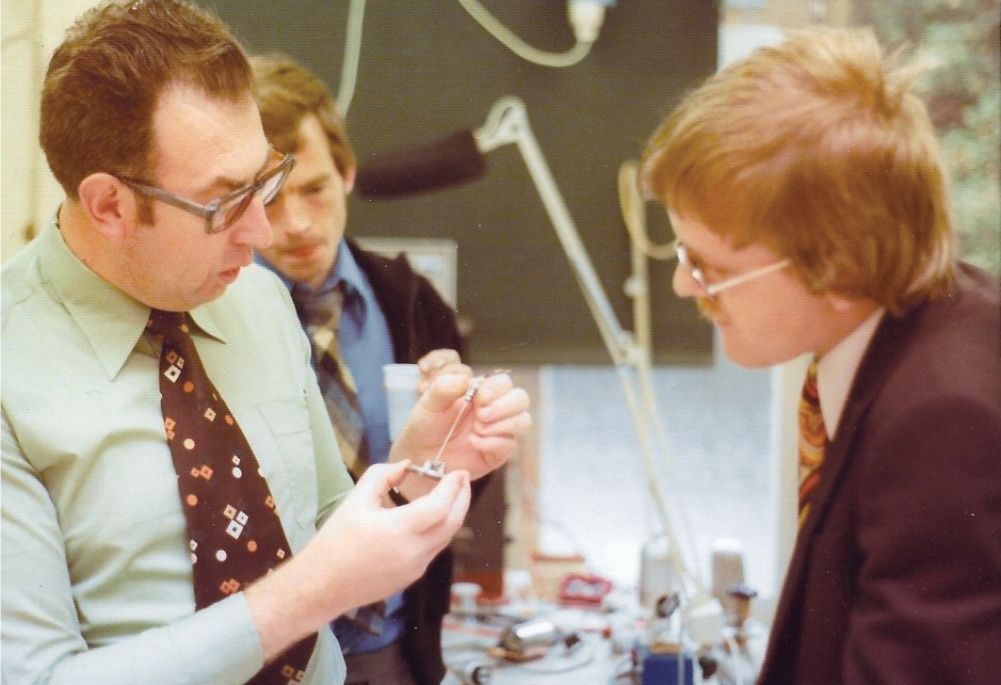
The first was engineer Martin van Beest, hired as ASM’s first employee in 1965 (see figure
Figure 3.

Martin van Beest (left) talks with colleagues in the 1970s. (Courtesy of ASM International.)
In the early 1970s, after a market downturn caused Applied Materials to withdraw from a planned joint venture with ASM to assemble such reactors in Europe, Del Prado decided to produce them internally. Van Beest was put in charge of that operation. He ordered the necessary components from companies across Europe and assembled the deposition reactor in fall 1971 in the attic of ASM’s headquarters in Bilthoven. Dubbed the SOX 10-2 because it could process 10 wafers, each with a 2-inch diameter, the reactor was ASM’s entry into the field of semiconductor equipment manufacturing.
Plasma-enhanced furnaces
In the 1970s Del Prado began to leverage the international appeal of Dutch technology and established ASM subsidiaries abroad. In 1975 ASM Asia was established in Hong Kong, and a year later ASM America was set up in Phoenix, Arizona. Those branches had to cultivate business autonomously from their Dutch parent. ASM America quickly hired several engineers who had formerly worked at Motorola, the largest US semiconductor company of the day. By 1978 ASM America succeeded in making limited inroads into the US market for horizontal chemical vapor deposition furnaces, which attracted the attention of the ambitious and hands-on engineer George Engle.
In the early 1970s, Engle was working for Applied Materials when he began using his spare time to tinker with chemical vapor deposition furnaces in his garage. At that time, researchers were increasingly interested in a new silicon nitride deposition process called plasma-enhanced chemical vapor deposition, which allowed the passivation of the latest chips at low temperatures. Yet such methods often produced impurities in the silicon or were uneconomical. Engle’s new type of horizontal deposition furnace proved to be just the solution. Instead of laying the silicon wafers flat in a heated tube, as was done in previous deposition furnaces, Engle stood them upright and placed them against graphite plates positioned longitudinally in the tube. He then ignited a plasma between the plates. His technique allowed the deposition of silicon nitride for passivation films to be carried out in large quantities.
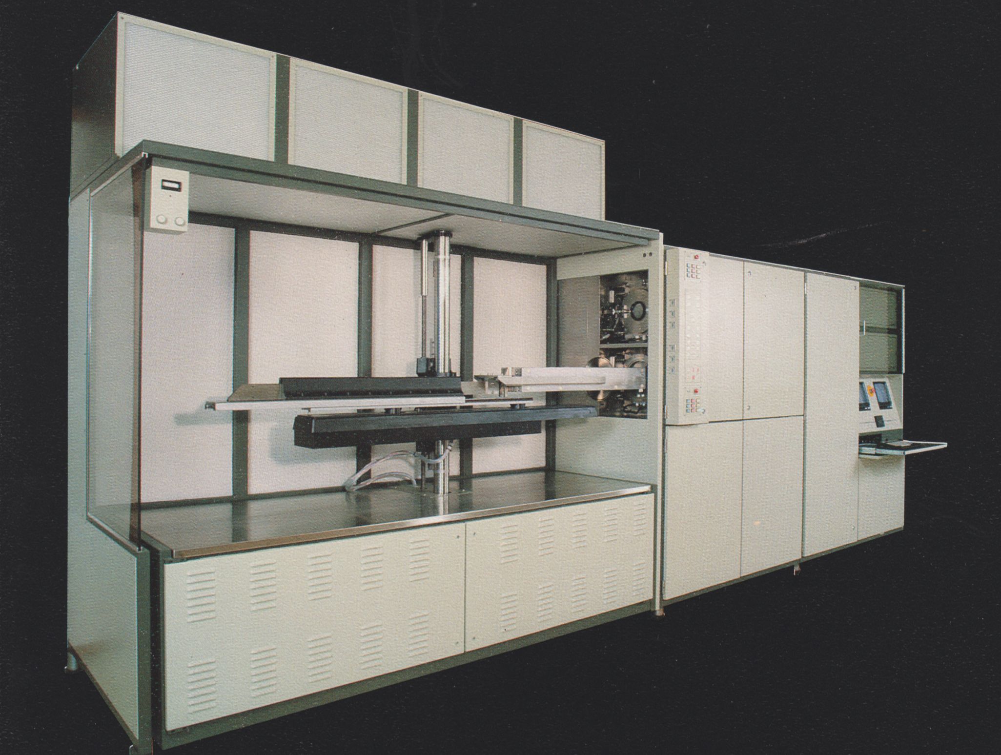
Convinced of his machine’s success, Engle peddled his ideas to his employer, but it turned him down. A rival firm, Pacific Western Systems, helped Engle build a few furnaces, but he was quickly dissatisfied by the company’s failure to market them aggressively. He soon took his patented idea to a more ambitious and audacious party: ASM America. Engle’s furnace was introduced by the subsidiary in 1979 as the Plasma I (see figure
Figure 4.

ASM America introduced the Plasma I reactor, designed by George Engle, in 1979. Shown here are the horizontal plasma furnace (right) and its loading station (left). (Courtesy of ASM International.)
In accordance with Del Prado’s management strategy, the funds from both the initial public offering and a subsequent flotation of shares in 1983 were leveraged to expand the company further. Time and again, ASM reinvested the capital it accrued from investments or profits into skilled and dedicated groups of engineers, who produced new innovations that fueled the company’s growth. In 1982 ASM Japan was established with a workforce of ambitious service engineers who knew the country’s market intimately. ASM Lithography (ASML), a joint venture with Philips, followed in 1984. That subsidiary was staffed with former Philips employees and complemented with an influx of intrepid and enthusiastic young engineers. 5
A year later a group of experienced engineers in ion-implant technology convinced Del Prado to fill a gap in that market, which led to the founding of ASM Ion Implant in Beverly, Massachusetts. More new divisions and subsidiaries followed. By the end of 1985, ASM had revenues of 351 million Dutch guilders (approximately $321 million in today’s dollars), a huge sum at the time. With 1870 employees across 13 divisions worldwide, the company was an international powerhouse in semiconductor equipment technologies.
Del Prado structured his company and its subsidiaries in decentralized divisions that operated autonomously. ASM was not one monolithic company; it was ASM Japan, ASM America, ASM Europe, ASM Fico, ASM Assembly Automation, ASML, ASM Microelectronics Technology Center, and more—all managed by a small, agile parent company called ASM International, of which Del Prado was the majority shareholder. Each new branch or subsidiary added to the plethora of ASMs.
Imperial overreach
Yet ASM’s expansion could not be sustained indefinitely. In the latter half of the 1980s, the company began to flounder. Following an industry downturn in 1984 and 1985, the dynamics of the international semiconductor market changed. As manufacturers began to specialize in specific market segments, such as microprocessors or memory, their needs diverged. Before, they had all sought the same technology—horizontal deposition furnaces—but now manufacturers wanted equipment tailored to the specific semiconductors they built.
Demand for types of semiconductor equipment was correlated with regional market tendencies. Memory producers in Japan, for example, requested vertical batch furnaces, which would maximize productivity in increasingly expensive clean rooms with limited floor space. Microprocessor and application-specific chip producers in the US, on the other hand, demanded single-wafer reactors that processed only one silicon wafer at a time but allowed for the higher process qualities needed to produce such chips.
Because of that market divergence, ASM’s organizational structure became increasingly obsolete. The multiplier effect resulting from selling horizontal deposition furnaces to manufacturers worldwide was gone. ASM’s various business units had to reinvent themselves while maintaining revenue. In doing so, they often found themselves interfering and competing with the business of other ASM divisions. Costs increased dramatically, which meant that less revenue remained to sustain leveraged innovation in lithography, in ion implantation, and at the company’s new research center.
ASM’s capability to organize promising engineers and technology proved to be too closely tied to a single person. Del Prado’s personality was a hindrance to the company’s ability to address changing market dynamics. He was unable or unwilling to impose a cohesive direction on ASM and rein in the company’s headstrong divisions. Moreover, he refused to relinquish complete control over the enterprise, which hampered its finances. To gain an influx of capital, Del Prado used conventional short-term loans to fund ASM rather than selling some of his shares, which would have dropped his stake in the firm below 50%. That decision could have worked only if all of ASM’s money-draining ventures quickly transformed into moneymakers—but they did not.
By 1988 the bleeding at ASM had to stop. The company began selling off some of its developmental ventures to improve its finances. It divested its share of ASML that summer and sold ASM Ion Implant to Varian Associates around the same time. In December the Hong Kong division was floated as an independent subsidiary on the Hong Kong Stock Exchange under the name ASM Pacific Technology, with ASM initially retaining a 75% stake in the venture.
Even that was not enough. As horizontal deposition furnaces became increasingly obsolete and ASM failed to develop profitable successors, the company’s finances continued to deteriorate. Between 1991 and 1993, practically all its remaining assets were up for sale. The research center was closed. ASM Fico, the European division that produced semiconductor encapsulation equipment, was eventually sold to Berliner Elektro Holding in fall 1993 and renamed BE Semiconductor Industries. Now known as Besi, the venture is one of ASM Pacific Technology’s main competitors.
ASM’s fragmented structure proved to be a blessing in disguise for its divested divisions. They had already operated with considerable independence, and now that they no longer needed to share funds with unprofitable divisions, the ventures prospered and grew. ASML is now the world’s leading supplier of lithographic equipment, and Besi and ASM Pacific Technology are market leaders in semiconductor assembly and packaging technologies. Del Prado’s ASM children continue to dominate the industry.
The tumultuous 1990s
Even though Del Prado’s leadership was partially responsible for the company’s failings in the late 1980s and early 1990s, he remained ASM’s founder, CEO, and majority shareholder. But he was forced to make changes. An interim manager, Ray Friant, was installed as chief operating officer to help with decision making. To turn around the company’s fortunes, Friant argued in a report that Del Prado, whom he acknowledged was a “visionary,” needed to be complemented by “practical business personnel who are focused on making money each month.” 6
Although some argued that Friant needed to streamline and centralize ASM’s operations, he chose to keep the fragmented structure that the company had developed under Del Prado. Instead, under his and Del Prado’s keen eyes, ASM retained its stake in the increasingly profitable ASM Pacific Technology while simultaneously focusing its business around three novel deposition technologies. Each of those methods were championed by one of ASM’s divisions: ASM Europe developed a novel vertical low-pressure deposition and diffusion furnace, ASM America offered customers a single-wafer epitaxial reactor, and ASM Japan marketed a single-wafer plasma deposition tool.
That allowed ASM’s fragmented structure to again work in the company’s favor, because it meant that each division could focus on a different product and therefore a separate market. Friant’s business acumen saved the company—and it was just in time, for by 1997 ASM needed to settle an escalating legal dispute with Applied Materials over epitaxial technology for the daunting sum of $80 million.
But a leopard can’t change its spots. With the lawsuit settled, Del Prado returned to his old playbook during the late 1990s dot-com bubble. Once again, he began to expand ASM into new markets. Now it was in the equipment segment for deposition technologies. In 1999 ASM acquired the Finnish company Microchemistry, which had developed promising atomic layer deposition technologies, processes, and tools. Such methods enable the layer-by-layer formation of thin films with nearly perfect conformality and step coverage across complex nanoscale geometries. Microchemistry’s engineers and scientists lacked practical experience in semiconductor manufacturing, but they were intimately familiar with the chemical processes it involved. Teaming up with in-house experts at ASM, they began a decade-long endeavor to commercialize atomic layer deposition.
History repeated itself at ASM. Although efforts were made to centralize semiconductor manufacturing, the company remained highly fragmented. Divisions like ASM Europe, ASM America, and ASM Japan—each with their respective technology—were largely left to themselves. All three enjoyed market success in the late 1990s and early 2000s, but their profits were eaten up by the company’s investments in newly acquired divisions like Microchemistry.
This time around hedge fund managers took aim at Del Prado’s strategy. Several of them had bought stakes in ASM, and from 2005 to 2013 those activist investors pushed for the company to sell off its remaining stake in ASM Pacific Technology. They even advocated for ASM itself to be put on the block. That period of shareholder activism coincided with Del Prado’s retirement at age 77 in 2008, after which his presence in the organization steadily decreased. He was succeeded by his eldest son, Chuck del Prado, whose appointment only added fuel to the hedge fund managers’ fire.
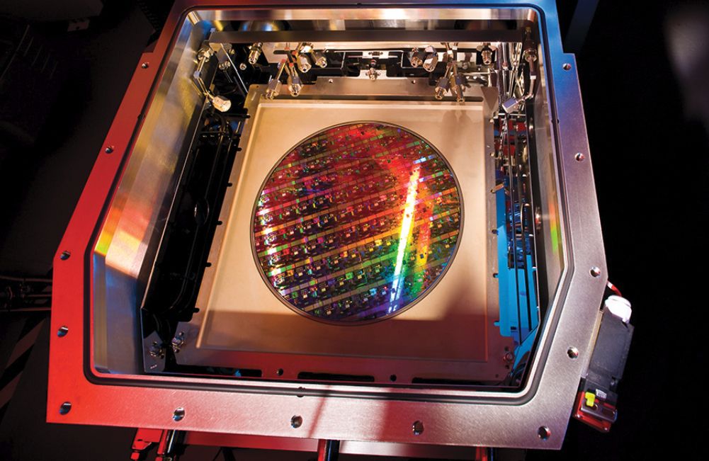
Like his father, Chuck was determined to keep the company intact. Fortunately for ASM, its acquisition of Microchemistry had begun to bear fruit in 2007, when it successfully introduced atomic layer deposition technology into high-volume chip manufacturing (see figure
Figure 5.

ASM International’s resurgence in the late 2000s was fueled by its investments in atomic layer deposition technology. This image depicts a wafer in part of a reactor that uses the technology to fabricate semiconductors. (Courtesy of ASM International.)
References
1. Semiconductor Industry Association, “Global Semiconductor Sales Increase 6.5% to $439 billion in 2020” (1 February 2021).
2. U. Pillai, Bus. Hist., 1 (2020), doi:https://doi.org/10.1080/00076791.2020.1844666 .
3. C. Lécuyer, D. C. Brock, Hist. Technol. 22, 301 (2006). https://doi.org/10.1080/07341510600803440
4. H. I. Ansoff, Harvard Business Review, September–October 1957, p. 113;
P. F. Drucker, Harvard Business Review, January–February 1967, p. 92;
P. F. Drucker, Harvard Business Review, January–February 1974, p. 45;
K. Sluyterman, Dutch Enterprise in the Twentieth Century: Business Strategies in a Small Open Economy, Routledge (2005), p. 164.5. R. Raaijmakers, ASML’s Architects: The Story of the Engineers Who Shaped the World’s Most Powerful Chip Machines, Techwatch Books (2018);
J. van Duijn, Fortunes of High Tech: A History of Innovation at ASM International, 1958–2008, Techwatch Books (2019).6. Ref. 5, J. van Duijn, p. 534.
More about the authors
Jorijn van Duijn is a historical consultant in Utrecht, the Netherlands. He received his PhD in innovation studies, business history, and technology history from Maastricht University in 2019. This article is based on his book Fortunes of High Tech: A History of Innovation at ASM International, 1958–2008 (2019).


