An Organic Electronics Primer
DOI: 10.1063/1.1995748
Interest in the electronic properties of semiconducting organic molecules dates back many decades to classic studies of ground- and excited-state electronic structure of model molecules, such as anthracene, performed in the early 1960s by Martin Pope and colleagues. 1 Since then, various semiconducting organic molecules and polymers have been steadily developed.
The use of organic semiconductors in xerography gave that field a particular boost during the 1980s (see the article by Joseph Mort in Physics Today, April 1994, page 32 ). As photoreceptor materials on photocopier and laser-printer drums, organics could generate and transport charge, usually as solid mixtures of molecular semiconductors in inert polymer hosts. The vast majority of copiers and laser printers now use those materials systems, and the underlying science has matured, especially in the context of industrial application. 2
Today, electronics researchers are more focused on reducing the size of semiconductor devices to their fundamental limits, where molecules play the active roles in circuitry (see the article by James Heath and Mark Ratner in Physics Today, May 2003, page 43 ). In that pursuit, the development of organic semiconductors—an activity loosely termed organic electronics—parallels the development of their inorganic cousins, such as silicon or germanium; the use of organics, molecular or polymeric, in devices has developed to the point of supporting consumer products. Organic light-emitting diode (LED) displays are, for instance, now commercially available.
Organic semiconductors have captured the interest of the electronics industry for good reasons. A wide range of properties, such as solubility in organic solvents and the color of light emission, can be finely tuned via chemical synthesis. The tunability facilitates the engineering of molecules to fit specific requirements. Another attractive feature involves processing (see the box on page 58). Polymer coatings can be easily applied over large areas and to a variety of substrates, including mechanically flexible ones. Associated with the ease of processing is the potential for low-cost fabrication. Arrays of pixelated organic LEDs have been extensively developed for application in high-performance displays, and large-area displays are now close to large-scale manufacturing.
However, low charge mobility compared to single-crystalline silicon, and other identifying characteristics, limit the range of applications envisioned for organics. Organic electronics is not meant to replace traditional silicon electronics, but rather to complement it and extend its capabilities.
The ground state
Carbon-based molecular semiconductors share a common structural feature: The bonding in the molecule or along the polymer backbone consists of alternating single and double carbon–carbon bonds. This alternation is termed conjugation. Double bonds form when the carbon atoms bond through sp2 hybrid orbitals, which produces three covalent σ bonds within a plane and leaves the out-of-plane pz orbitals nonhybridized. Overlap of pz orbitals on adjacent carbons can form π orbitals, which are substantially delocalized over the molecule or along segments of the polymer chain. The filled π bonding orbitals form the valence states, and the empty π* antibonding orbitals form the conduction states.
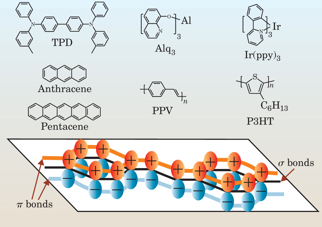
Graphite is one example of a conjugated material, although in that case, partial overlap of conduction- and valence-band states results in a semimetal. Figure 1 shows a range of conjugated molecules and polymers. Many of the now important molecular materials were developed first in electrophotography, whereas conjugated polymers, such as poly(phenylene-vinylene), or PPV, were first studied for their use in doped states as conducting materials, work that earned Alan Heeger, Alan MacDiarmid, and Hideki Shirakawa the Nobel Prize in Chemistry in 2000. 3 (See Physics Today, December 2000, page 19 .)

Figure 1. A gallery of organic semiconductors. These delocalized-electron systems can be identified by their alternating single and double carbon–carbon bonds. Molecular materials such as TPD, Alq3, and Ir(ppy)3 are widely used in LEDs, and pentacene and others in FETs. Polymer semiconductors have π molecular orbitals along the main chain and are also used in LEDs (PPV) and in FETs (P3HT). The bottom panel is an artist’s impression of the π molecular orbitals on a PPV chain segment. To form the molecule, an sorbital for each carbon atom becomes mixed with two of the p orbitals (sp2 hybridization), resulting in the σ bonds (black) that hold the molecule together. This leaves one electron per carbon atom in a pz orbital. The overlap of the pz orbitals (red and blue) of neighboring carbon atoms allows the delocalization of those electrons into π orbitals along the polymer backbone.
In molecular semiconductors, transporting charge between molecules requires adequate overlap of the π orbitals on adjacent molecules. Such overlap generally occurs for conjugated molecules because the chemical bonding forces the structure to be planar. Carbon-60 and other fullerenes are the exceptions. The packing of molecules in the solid state can provide good contact between the π wavefunctions, which are relatively extended on either side of the plane of the molecule; a crude measure of this intermolecular π–π contact within a tight-binding description of the electronic structure is the strength of the resonance or transfer integral, generally about 0.1 eV for well-ordered materials.
For polymers, in which the π-electron system is delocalized along the backbone, intrachain widths of the π valence and π* conduction bands are considerably higher: Values for the transfer integral can reach 1–3 eV. The delocalization promotes much easier intrachain charge transport, although interchain transport is still required for the usual size range of devices made using polymer semiconductors.
Well-delocalized conduction- and valence-band states are required for useful semiconducting behavior. An important feature is the presence of the σ single bonds formed by the sp2 hybrid orbitals. Those bonds are much stronger than the π bonds and can hold the molecule intact even in the presence of π-electron excited states—electrons, holes, and excitons (bound electron–hole pairs).
Disorder plays an important role in organic semiconductors, but its nature and impact on electronic properties differ dramatically from those of inorganic semiconductors. Disorder is commonly found in noncrystalline organization of molecular semiconductors and in the conformation of polymer chains. Disorder in the organics, unlike in inorganic semiconductors, is not usually associated with broken chemical bonds, because covalent bonds within molecules or polymer chains remain intact. As we discuss later, that feature makes possible very clean interfaces between dissimilar organic semiconductors.
Disorder does, however, strongly affect the transport properties of organic semiconductors insofar as it can localize charges and excitons on lattice sites. That is sometimes used to good effect, particularly in thin-film LED structures, but is problematic for devices such as FETs that require high charge mobilities to work well.
Excited states
The electronic excitations of molecular semiconductors can be modeled either from a molecular description, in which the excitation is presumed at the outset to be substantially confined or localized on an individual molecule, or from a band perspective, which uses delocalized wavefunctions to describe the behavior. What makes molecular semiconductors complex is that their behavior often stands at the crossover between those contradictory localized and bandlike descriptions.
Consider some basic observations. Molecular semiconductors have low dielectric constants, typically around 3, so screening of Coulomb potentials is relatively weak. Consequently, the Coulombic attraction between a photoexcited electron and hole binds them strongly. This description of the exciton is a useful starting point for understanding the character of optically excited states. If one sets the electron and hole effective masses to the free-electron mass and uses a dielectric constant of 3, the resulting exciton hydrogenic binding energy is about 0.75 eV and the Bohr radius is about 0.3 nm. That spatial size is at the limit where the excited state is confined to an individual molecular unit.
Because the exciton is so strongly localized on an individual molecule, a substantial energy difference or “exchange energy” exists between spin-singlet and spin-triplet exciton configurations. The difference is comparable in magnitude to the Coulomb binding energy, commonly in the range of 0.5–0.7 eV. In the absence of spin–orbit coupling, radiative emission from the triplet exciton is forbidden; that makes triplet formation through electron–hole capture detrimental to efficient LED operation.
Although singlet and triplet excitons are presumed to extend over roughly the same volume in molecular materials, their role in conjugated polymers is more complex. Singlet excitons in polymers are relatively delocalized along the chain and extend up to 10 nm in well-ordered materials, whereas triplet excitons, with their spatially antisymmetric wavefunctions, are much more localized.
A second general consequence of localized excited states on molecular semiconductors is their effect on electron–lattice interactions and thus on the local band structure. In simple terms, confining the antibonding wavefunction—produced by moving an electron from a π valence-band state to a π* conduction-band state—to a small number of carbon–carbon bonds causes substantial rearrangement of the valence electrons. The local bond lengths change in response to that rearrangement and prompt concomitant changes in both optical absorption and luminescence.
For polymer chains that contain benzene units, it is the normally Raman-active ring-stretching mode that is vibrationally coupled to the electronic transitions in the material. Such high-energy vibrational modes are often seen as distinct peaks in both light-absorption and emission measurements.
Charges, crystals, and chains
Electrons and holes in π* and π states can have moderately high mobilities, though the motion depends on the nature of the disorder in the sample. Norbert Karl and colleagues at the University of Stuttgart carried out the classic measurements of carrier mobility on single crystals of naphthalene. 4 At room temperature, they found mobilities of about 1 cm2 per volt-second. As temperature falls, charge mobility rises rapidly, reaching as high as 300 cm2/Vs at around 10 K. Below 100 K the mobility’s dependence on temperature T scales as T −1.5, characteristic of electron–phonon scattering through an acoustic deformation potential. In that regime, electrons behave like free carriers.
The mobility of electrons or holes in amorphous organic semiconductors such as molecular glasses and solid mixtures of conjugated molecules in polymers is far lower—typically 10−6 to 10−3 cm2/Vs—and depends strongly on the applied electric field. The randomness in the molecular positions and orientations leads to strong localization of carriers on individual molecules, and the transport takes place by charges hopping between molecules. 2 The absence of grain boundaries and the fact that the amorphous state is not associated with distorted or broken bonds means that trap-free charge transport can occur, a key requirement in electrophotography.
Studies of transport in amorphous organics have led to the development of the Gaussian disorder model by Heinz Bässler of the University of Marburg. According to that model, charges move by hopping between localized energy states with a Gaussian density of states.
Another aspect of electron–lattice interactions to consider is that of polaron formation, by which the lattice is locally deformed by the presence of an excited electronic state. The contribution of this electron–lattice interaction to the self-localization of electronic excited states in polymers has been beautifully modeled in terms of relatively extended excitations of the ground-state π electrons. Wu-Pei Su, Robert Schrieffer, and Heeger showed that the particular bond-order symmetry of the trans-isomer of poly-acetylene has the potential to support soliton-like excitations. A charge and the lattice deformation that accompanies it can move through a polymer chain as a solitary wave, or soliton (for a recent discussion of solitons, see Physics Today, January 2004, page 43 ). 3
More generally, symmetry considerations—that is, constraints on how bond lengths may rearrange—allow only polaron excitations on polymers such as P3HT (poly-[3-hexylthiophene]) and PPV, pictured in Figure 1. An electronic charge placed on a perfect polymer chain self-localizes to form a polaron. The literature is not consistent about the strength of that localization: Experiments that probe the electronic structure of chemically doped materials—so-called charge-transfer complexes with ions present alongside the polymer chain—indicate that it is strong, whereas experiments with field-induced charges argue for much weaker localization. Disorder plays an important role: Strong Coulombic potentials from the disordered ions localize the charge-carrier wavefunction on the chain, and thus contribute to a local geometric reorganization.
Light-emitting diodes
Diode structures can be manufactured by successive deposition of organic and inorganic layers, either by vacuum sublimation of molecular semiconductors 5 or by solution processing—“spin-coating,” or the direct printing of polymer solutions. 6 Many simple diode structures function as LEDs, and the efficiencies, durability, and color control of those devices have led to commercial products such as large pixelated displays.
Organic LEDs operate through electron and hole injection from opposite electrodes, electron–hole capture within the bulk of the semiconductor film to form bound excitons, and subsequent radiative emission from those excitons. That the devices work at all, let alone very efficiently, has come as a surprise: The organic semiconductor layers are generally thin—about 100 nm—and one might expect the interfaces between the layers and the two inorganic electrodes to be troublesome. Indium tin oxide on a transparent support substrate—usually glass, but sometimes polymer—is generally used as the bottom, hole-injecting electrode, although coating it with hole-transporting organic layers can improve performance. Low work-function metals are required for electron injection, and calcium or magnesium, often alloyed, are metals widely used.
Figure 2 shows an energy-level diagram for an organic LED. The crude model is moderately successful because the interfacial chemistry at both electrodes is relatively benign—that is, the metal–organic interface, rather surprisingly, does not introduce broken bonds with energy states deep in the semiconductor gap. That chemistry has, however, become a rich area of investigation of chemical reactions and charge polarization at interfaces. Photoelectron spectroscopy has proven to be a very powerful technique, as used by William Salaneck at Linköping University in Sweden, Antoine Kahn at Princeton University, and Kazuhiko Seki at Nagoya University in Japan, and complemented by quantum chemical modeling, particularly by Jean-Luc Bredas and his group at Mons, Belgium, and at the Georgia Institute of Technology. 7

Figure 2. The energy level diagram of an organic semiconductor LED (top), formed from two semiconductor layers set between an anode that injects holes and a cathode that injects electrons. The properties of the heterojunction formed between the two semiconductors are determined by the different energies of highest occupied (valence-band) state and lowest unoccupied (conduction-band) state across the junction. Those energy levels can be tuned by selecting appropriate materials. Of the two polymers shown in the middle panel, the shaded triphenylamine group in TFB is a good electron donor. The shaded benzothiadiazole group in F8BT is a strong electron acceptor. F8BT thus has a high electron affinity or low-lying conduction-band edge. The energy offsets in the conduction and valence bands block injected holes and electrons from reaching the opposite electrode. That promotes electron–hole capture and exciton formation at the heterojunction. The effect of the two polymeric semiconductors is to produce an efficient LED with green-yellow emission at efficiencies greater than 20 lumens per watt. The emission spectrum (bottom) from a TFB–F8BT heterojunction shifts to lower wavelengths with increasing temperature as interfacially trapped excitons migrate into the bulk of F8BT. The black dots signify emission from the F8BT polymer alone.
(Adapted from ref. 8.)

Most effective LED structures incorporate at least one heterojunction between different organic semiconductors to control and balance electron and hole currents and the electron–hole recombination zone. Ching Tang and Steven Van Slyke first demonstrated the efficacy of that approach in 1987 at Kodak 6 by using vacuum sublimation of hole-transporting TPD (triphenyl diamine derivative) onto an indium tin oxide anode, followed by a layer of electron-transporting Alq3 (aluminum tris[8-hydroxyquinoline]). Both the conduction and valence bands of the Alq3 are displaced to lower energies than those of the TPD in the heterostructure. The band-edge offsets block the migration of electrons and holes across the heterojunction; the effect is to confine the electron–hole recombination close to the organic/organic interface. LEDs with very high efficiencies—above 20 lumens per watt in the green part of the visible spectrum—can now be manufactured using that architecture.
The substantial exciton binding energy determines the electronic processes at and near the heterojunction. In the absence of that binding energy, an exciton present at the heterojunction would be unstable against charge dissociation. The electron would migrate to the lower-energy conduction-band state on the right, and the hole to the higher-energy valence-band state on the left. However, that process of exciton ionization (or, in the context of photo-excitation, photoinduced charge transfer) can occur only when the band-edge offsets are larger than the exciton binding energy. Since exciton ionization is undesirable for an LED, the goal is to select organic materials that allow the exciton to remain stable at the heterojunction.
Recently, using heterojunction devices made from TFB and F8BT, two polyfluorene polymers that form a film from xylene solution, researchers from the University of Cambridge investigated the nature of the electron–hole capture process and the energetics of the exciton near the heterojunction. 8 An electron and a hole that are opposite each other at the heterojunction form an interchain “charge-transfer exciton.” Subsequently, this defect becomes converted through barrier-free interchain tunneling to a substantially intrachain exciton centered on the lower-gap F8BT. Furthermore, the contact across the heterojunction allows this bound exciton to lower its energy by becoming somewhat delocalized across the heterojunction.
A redshift of about 140 meV in the device’s emission is a sign that the exciton has become trapped at the heterojunction, as is a much increased radiative lifetime—from 2 to about 100 ns—of the exciton on the F8BT side of the heterojunction. It takes low temperatures to see the redshifted emission, though, because higher temperatures excite the exciton into the material’s bulk, where it regains its oscillator strength and can find a faster radiative emission pathway.
Triplet excitons also play an important role in LED operation. As discussed earlier, triplet excitons are generally 0.5–0.7 eV lower in energy than the corresponding singlet and, once formed, are unlikely to decay radiatively in simple hydrocarbon organic semiconductors. Assuming that electron–hole capture is spin-independent, only one in four capture events produces a singlet, which is a severe limitation to efficiency if the other three triplet excitons are nonemissive. But Mark Baldo and Steven Forrest at Princeton and Mark Thompson at the University of Southern California have shown that an organometallic complex incorporated into devices can act as the emissive site; that work has produced major improvements in device efficiency. The substantial spin–orbit coupling can allow both singlet and triplet excitons to emit radiatively. 9 Complexes made from iridium—tris(2-phenylpyridine)iridium or Ir(ppy)3, for instance, whose structure is pictured in Figure 1—have been particularly successful in boosting efficiencies in the green and red portions of the spectrum.
Photovoltaic diodes
Exciton energetics can be engineered through the judicious choice of materials in heterojunction schemes: By making the energy difference between valence- and conduction-band levels across the heterojunction sufficiently large, the energy advantage of separating electrons and holes outweighs the Coulomb binding energy of electron and hole in an exciton. For a review of such systems, see reference . When constructed as two-layer abrupt heterojunctions, systems such as the one shown in Figure 2 are relatively inefficient because photogenerated excitons must reach the junction interface to ionize. And their characteristic diffusion range is generally only 10% or so of the thickness of material required for full optical absorption.
One promising approach to the problem is to form a “distributed heterojunction” structure, which allows all photogenerated excitons to be sufficiently close to heterojunctions that they can readily diffuse there and thus be ionized. Researchers working at the University of California, Santa Barbara, and Cambridge University first developed that approach in work that has now produced promising values of photovoltaic performance; energy conversion efficiencies are above 3% for materials systems whose absorption spectra are still not well matched to the solar spectrum. 11
Field-effect transistors
Field-effect structures such as transistors are now routinely made using organic semiconductors. 12 Applying an electric field across the dielectric layer through control of the gate voltage induces a surface charge density at the interface between an organic semiconductor and a suitable dielectric. The induced charge density provides the conduction path between source and drain electrodes. Figure 3 shows a commonly used transistor structure. A doped silicon wafer provides the gate electrode, thermally grown silicon dioxide serves as the dielectric layer, and lithographically patterned gold forms the source and drain. Completing the transistor requires only depositing the organic semiconductor by sublimation or by solution processing.

Figure 3. Structure of a field-effect transistor. (a) A thin organic layer covers an insulating surface with gold source and drain electrodes on either side. (b) A height profile across the device shows 200-nm steps at those electrodes and the 5-micron-wide channel. (c) With an electron-doped silicon gate biased at −20 V, a scanning probe measures the potential drop across the channel as a function of various source–drain voltages, Vsd.
(Adapted from ref. 13.)
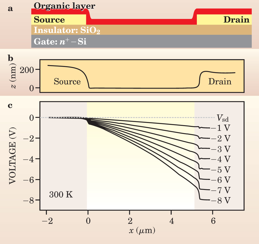
The transistor’s open structure makes it amenable to direct probing of the electric potential across the source–drain channel. Daniel Frisbie (University of Minnesota), Thomas Jackson (Pennsylvannia State University), and Lukas Burgi and Henning Sirringhaus (Cambridge) have directly observed device operation using, for example, a Kelvin probe 13 that scans the potential on a film of P3HT (poly[3-hexylthiophene]) at a range of source–drain voltages. The scans show the expected variation of potential across the channel, but they also reveal that there can be significant contact resistances, with voltage drops at the electrodes—in this example, both for charge injection and for extraction. Contact effects due to polarization at the metal–organic semiconductor interface, 8 for instance, are now relatively well characterized, and a number of methods exist that avoid such substantial voltage drops. 14
The mobilities of the field-effect charges determine the usefulness of the device for both research and applications. The challenge in materials processing is to achieve a well-ordered interface between semiconductor and dielectric, because the surface-induced charges are confined near that interface. Treating the top SiO2 surface chemically—to replace the polar SiO2 surface with a sheet of alkyl chains (C n H2n+1), for instance—greatly improves the order. Mobilities for the best-ordered polymers, such as P3HT, can be made as high as 0.1–0.2 cm2/Vs. For those polymers, the mobility is too high to be described in terms of a hopping model between disorder-localized states and is at the threshold of bandlike behavior.
In light of that relatively high mobility, to what extent are polaron models, widely used for chemically doped conducting polymers, 3 applicable? One experimental approach is to measure the change in optical absorption through an FET or diode as the field-induced charge concentration is modulated by the gate voltage. In chemically doped polymers, evidence exists for localized polarons with local π bonding (see the schematic representation in Figure 4). Conduction- and valence-band states move into the bandgap in response to distortions in the lattice caused by the presence of polarons. Spectroscopically, one sees strong optical absorption bands emerge deep in the semiconductor gap. 3

Figure 4. A positively charged polaron associated with the presence of a hole can be represented by a local change in the chemical structure (a) along a section of a polythiophene chain. To accommodate the hole, the chain alters its bonding pattern, shown schematically here over a length of 4 thiophene units. (b) Such localized defects in bonding prompt the valence- and conduction-band states to move into the energy gap. The changed energy states are manifest as new absorption bands at 0.5 eV (C1) and 1.3 eV (C2). (c) The change in those energy levels can be measured as a change in optical transmission −ΔT through an FET when the gate voltage is applied. Plotted as −ΔT/T, the positive signals correspond to induced absorption, as seen below 2 eV, and the negative signals to “bleaching,” the loss of ground-state bands above 2 eV. The transmission spectrum changes on well-ordered polythiophene-based films (P3HT) with field-induced charge doping are characteristic of delocalized free charges. The weaker contributions from the C1 and C2 polaron bands are associated with chemical doping.

The strong localization is associated with the presence of dopant ions. However, in the field-effect device, charges are introduced by themselves, and the differential absorption spectra plotted in Figure
Molecular semiconductors such as pentacene compare favorably to the field-effect mobility in amorphous silicon transistors (1 cm2/Vs). The physical limits to mobility are not clearly understood, although the relatively narrow bandwidths expected from the intermolecular π-electron interactions will restrict mobilities to values lower than those found in three-dimensionally bonded semiconductors. Values up to 15 cm2/Vs were recently reported for rubrene single crystals at room temperature. 16 The main challenges lie in understanding and controlling the growth of these materials to achieve films with well-defined structure and morphology—and in understanding the molecular origins of charge traps and other defects that molecular semiconductors contain.
Processing organic semiconductors
As soft materials with only van der Waals intermolecular interactions, molecular and polymeric materials must be processed in ways that differ dramatically from crystalline semiconductors like silicon. Indeed, much of the interest in organics has focused on finding new ways to form useful structures for devices. 17 Processing from the liquid phase is particularly appealing, because the method is scalable to large areas and can also allow direct patterning on a substrate.
But solution processing is of limited use for making molecular semiconductors because they often have limited solubility and do not form continuous thin films, tending instead to crystallize. When organics are solution-processed for use in electrophotography, they are dispersed within a polymer matrix. 2 In contrast, vacuum sublimation at relatively modest temperatures has proven very successful in forming high-quality thin films. The successive deposition of different molecular layers is straightforward, and hetero-structures made that way play an important role in LED and photovoltaic diode operation. Another virtue is that sublimation can be used as an effective purification procedure.
For polymers, solution processing is attractive for several reasons. It is convenient, can form thin high-quality films, and can allow molecular-scale organization of one material on another. A polymer layer can align onto a pre-ordered substrate via, for instance, a liquid-crystal mesophase; that is desirable in the case of FETs. The method can also allow complex morphologies with nonplanar interfaces between different semiconductors; one example is the use of controlled demixing of two polymers deposited from a common solution to form an interpenetrating network. The scanning force microscope image (at 50 microns on each side) shows the phase-separated blend of two polymers, PFB and F8BT, processed from xylene solution. The demixing process can be precisely controlled to form beautiful and elaborate di- and tri-block polymers (see the article by Frank Bates and Glenn Fredrickson, Physics Today, February 1999, page 32 ).
Semiconducting or conducting (doped semiconducting) polymers may also be formulated as “inks”—fluids that differ from each other in viscosity and surface tension—to be compatible with convenient printing methods. Ink-jet printing has proven especially popular as a practical way to pattern the red-, green-, and blue-emitting semiconductors required to make full-color LED displays. But it can also be used to print transistors and active circuits, with polymers used as semiconductors, insulators, and metals. By altering the surface free energy of the substrate, researchers can accurately steer the flow of fluid droplets on a circuit or substrate to some predetermined position. For a review of such applications, see reference .

Outlook
Progress in organic electronics is likely to closely follow advances in our understanding of the fundamental properties of organic materials. The underlying science is tremendously exciting: Weak intermolecular interactions, low dielectric constants, and the presence of disorder are characteristics that make organic semiconductors distinctive systems for exploring a variety of solid-state phenomena. And the availability of an unlimited number of different molecules represents the ultimate degree of freedom for the experimentalist and the best reason for using organics to study semiconductor physics. The technological groundwork that is being established with the commercialization of organic LEDs should guarantee a bright future for organic electronics.
References
1. For a review, see M. Pope, C. E. Swenberg, Electronic Processes in Organic Crystals and Polymers, 2nd ed., Oxford U. Press, New York (1999).
2. P. M. Borsenberger, D. S. Weiss, Organic Photoreceptors for Imaging Systems, M. Dekker, New York (1993).
3. A. J. Heeger et al., Rev. Mod. Phys. 60, 781 (1988) https://doi.org/10.1103/RevModPhys.60.781 .
4. N. Karl, in Organic Electronic Materials, R. Farchioni, G. Grosso, eds., Springer, New York (2001).
5. C. W. Tang, S. A. Van Slyke, Appl. Phys. Lett. 51, 913 (1987) https://doi.org/10.1063/1.98799 .
6. R. H. Friend et al., Nature 397, 121 (1999) https://doi.org/10.1038/16393 .
7. W. R. Salaneck et al., eds., Conjugated Polymer and Molecular Interfaces: Science and Technology for Photonic and Optoelectronic Applications, M. Dekker, New York (2002).
8. A. C. Morteani et al., Adv. Mater. 15, 1708 (2003) https://doi.org/10.1002/adma.200305618 .
9. M. A. Baldo et al., Appl. Phys. Lett. 75, 4 (1999) https://doi.org/10.1063/1.124258 .
10. B. A. Gregg, J. Phys. Chem. B 107, 4688 (2003) https://doi.org/10.1021/jp022507x .
11. H. Hoppe, N. S. Sariciftci, J. Mater. Res. 19, 1924 (2004) https://doi.org/10.1557/JMR.2004.0252 .
12. C. D. Dimitrakopoulos, P. R. L. Malenfant, Adv. Mater. 14, 99 (2002).https://doi.org/10.1002/1521-4095(20020116)14:2<99::AID-ADMA99>3.0.CO;2-9
13. L. Bürgi, H. Sirringhaus, R. H. Friend, Appl. Phys. Lett. 80, 2913 (2002).
14. Y. Shen et al., ChemPhysChem 5, 16 (2004) https://doi.org/10.1002/cphc.200300942 .
15. H. Sirringhaus et al., Nature 401, 685 (1999) https://doi.org/10.1038/44359 .
16. V. C. Sundar et al., Science 303, 1644 (2004) https://doi.org/10.1126/science.1094196 .
17. S. R. Forrest, Nature 428, 911 (2004) https://doi.org/10.1038/nature02498 .
18. H. Sirringhaus, T. Shimoda, Mater. Res. Soc. Bull. 28, 802 (2003) https://doi.org/10.1557/mrs2003.228 .
More about the authors
George Malliaras is a professor of materials science and engineering at Cornell University in Ithaca, New York. Richard Friend is the Cavendish Professor of Physics at the University of Cambridge in the UK.
George Malliaras, Materials Science and Engineering, Cornell University, Ithaca, New York, US .
Richard Friend, University of Cambridge, US .


